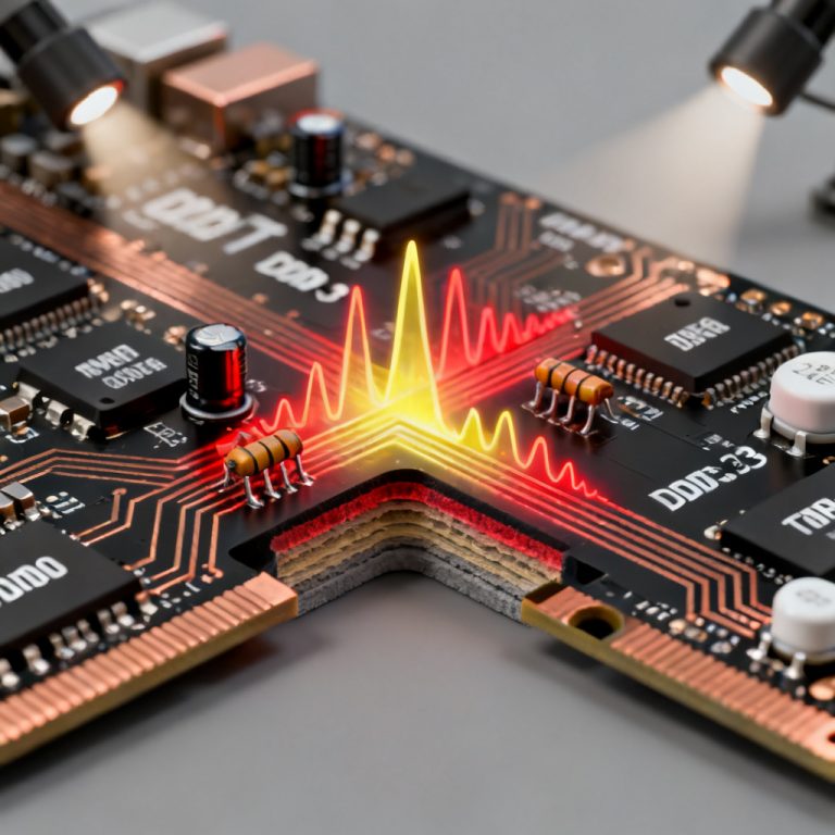
Return path design is as critical as signal trace routing for high-speed PCBs. This return path PCB guide explains signal return current, reference plane continuity, stitching vias, and EMI control based on industry standards. Part of our comprehensive Signal Integrity Guide.
Table of Contents
- 1. What Is a Signal Return Path
- 2. Why Return Path Matters for Signal Integrity
- 3. High-Frequency vs Low-Frequency Return Current
- 4. Reference Plane: Foundation of Return Path
- 5. Golden Rule: Never Cross Split Planes
- 6. Layer Transition & Stitching Via Design
- 7. GND to VCC Reference Plane Switching Rules
- 8. Return Path for Differential Pairs
- 9. Common Return Path Mistakes & Fixes
- 10. Return Path Discontinuity & EMI Antenna Effect
- 11. How to Verify Return Path in Layout
- 12. Key Takeaways
- 13. FAQ
- 14. Free PCB Return Path Design Review
What Is a Signal Return Path in PCB Design?
A PCB signal return path is the conductive path that allows electric current to flow back to the source, forming a closed electromagnetic loop for every signal trace. A common misconception is that return paths carry only DC current. At high speed, the returning flow is dominated by displacement current driven by alternating electromagnetic fields, not conventional DC conduction current. Return path PCB integrity directly determines signal quality, EMI levels, and system reliability.
Low-frequency return current spreads randomly by resistance, while high-frequency return current concentrates directly under the signal trace to minimize inductance. Without continuous return path continuity, even perfect trace routing will suffer reflection, crosstalk and excessive EMI. For deeper understanding of impedance, refer to our Impedance Matching Ultimate Guide.
Why Return Path Design Matters for High-Speed Signal Integrity
A core design principle: signal integrity equals forward trace integrity plus return path integrity. The return path is equally important as the signal route itself. Any return path PCB discontinuity leads to three critical issues:
- Higher EMI radiation from enlarged current loop area
- Increased crosstalk between adjacent high-speed traces
- Signal delay, jitter, waveform distortion and impedance reflection
| Item | Good Return Path | Poor Return Path |
|---|---|---|
| Reference Plane | Full solid GND/VCC plane | Split, hollow or cutout plane |
| Current Loop | Compact minimal area | Large detoured loop |
| Performance | Low inductance, stable impedance | Impedance discontinuity, high noise |
| SI & EMI | Low crosstalk, low radiation | 3 to 5 times higher EMI, obvious jitter |
High-Frequency vs Low-Frequency Return Current in PCB
The typical frequency boundary is 1MHz. Below and above this threshold, return current behaviors are completely different. For signals above 1MHz, always design return path PCB using high-frequency rules.
Low Frequency (<1MHz): Return current follows the lowest resistance path, spreading widely across ground and power planes. Loop area has little impact on low-speed performance.
High Frequency (>1MHz): Return current follows the lowest inductance path. Due to skin depth effect, current gathers tightly on the reference plane directly beneath the signal trace. This tight distribution keeps loop inductance low, stabilizes impedance and restricts electromagnetic radiation.
Reference Plane: The Foundation of PCB Return Path
Reference planes are solid GND or VCC copper layers in PCB stackups. They act as the main carrier for high-speed return current, provide stable low-inductance paths, maintain controlled impedance and suppress inter-layer crosstalk. Return path PCB design requires that high-speed signals always route above an unbroken solid reference plane.
| Plane Type | Return Path Status | Impact |
|---|---|---|
| Full Solid Plane | Uninterrupted direct return | Stable impedance, low EMI, minimal crosstalk |
| Split Plane | Current detours around gaps | Impedance jump, 3 to 5 times EMI increase |
| Hollow/Cutout Plane | Local return path blocked | Signal reflection, crosstalk hotspots |
Golden Rule: Never Cross Split Planes for Return Path Continuity
The most important rule for high-speed PCB design: Never route high-speed traces across split ground or power planes. When a trace crosses a plane split, return current cannot flow directly underneath. It must detour around the gap, greatly expanding the current loop. A larger loop acts as a natural antenna, causing EMI compliance failure. Return path PCB designs that cross splits raise noise and EMI by 3 to 5 times.
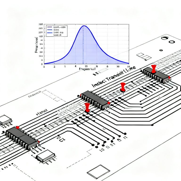
Layer Transition & Stitching Via Design for Return Path
When a high-speed signal switches layers via a signal via, its return path must also switch to the corresponding reference plane. The standard solution is ground stitching vias. Return path PCB rules require stitching vias within 30–40 mils from high-speed signal vias.
- Place stitching vias ≤30–40 mils from signal vias
- Use dense via fencing for high-speed buses (DDR, PCIe)
- Always add stitching vias for any high-speed layer transition
Rule of thumb: Distance ≤ 1/10 of the signal rise time spatial wavelength → for 1-10Gbps, ≤40 mils.
GND to VCC Reference Plane Switching Rules
In complex stackups, signals switch reference from GND to VCC planes. VCC planes cannot provide direct low-inductance AC return paths. Return current completes the transition through high-frequency decoupling capacitors (0.01μF or 0.1μF MLCC).
Return path PCB with VCC reference must include capacitors within 20–30 mils for core rails (1.2V/1.8V) or combine 0.1μF & 1μF for I/O rails (3.3V/5V).
Return Path for Differential Pairs in High-Speed PCB
Differential pairs have unique return characteristics: the two complementary traces act as mutual return paths, naturally suppressing common-mode noise. Tightly coupled pairs concentrate return current between the two traces, while loosely coupled pairs spread return current into the reference plane. Even with inherent noise cancellation, a solid reference plane is essential. See Differential Pair Routing Guide for complete rules.
Common Return Path Mistakes & Fixes
| Design Mistake | Consequence | Correct Solution |
|---|---|---|
| High-speed traces crossing split planes | EMI over-limit, jitter | Route only over solid reference planes |
| Layer transition without stitching vias | Broken return path, high inductance | Add GND stitching vias within 30–40 mils |
| Oversized reference plane cutouts | Impedance mutation, current detour | Minimize cutouts; add ground bridge stitching |
| VCC reference without decoupling caps | Interrupted AC return path, reflection | Place 0.01μF/0.1μF caps at reference switching points |
Return Path Discontinuity & EMI Antenna Effect
Every signal-return current loop works as a loop antenna. Radiation strength follows E ∝ I × A × f² (E=EMI intensity, I=current, A=loop area, f=frequency). Due to the f² relationship, high-speed GHz signals are extremely sensitive to loop area growth. The core EMI control strategy is to minimize return current loop area.
How to Verify Return Path in PCB Layout
Design Phase: In Altium, Cadence, enable reference plane visibility and check splits, gaps before routing. Use return path DRC rules. Simulation & Testing: Use SI/PI tools to analyze return current density; near-field probe scanning locates EMI hotspots.
Key Takeaways for Return Path PCB Design
- Return path performance is as important as signal trace routing
- High-frequency return current follows lowest inductance path directly under the signal trace
- The 1MHz rule: Above 1MHz, always use high-frequency return path design rules
- Never route high-speed signals across split reference planes
- Add stitching vias within 30–40 mils for all high-speed layer transitions
- Use decoupling caps when switching reference from GND to VCC
- Minimizing loop area is the key to EMI suppression
Return to Signal Integrity Guide for more in-depth coverage of impedance control, differential pairs, and via stub effects.
Frequently Asked Questions About Return Path PCB
What is a PCB signal return path?
A PCB signal return path is the closed conductive path for current returning to the source, forming a complete electromagnetic loop for signal traces. High-speed return flow is mainly displacement current.
Why avoid split plane crossing in return path design?
Split plane crossing forces return current to detour, enlarges loop area, increases EMI by 3 to 5 times, and causes jitter and signal reflection.
How to place stitching vias correctly for return path continuity?
Place stitching vias within 30–40 mils of high-speed signal vias to maintain continuous low-inductance return paths during layer transition.
Can VCC plane be used as return reference?
Yes, but you must place 0.01μF or 0.1μF decoupling capacitors nearby to provide AC short between GND and VCC.
Do differential pairs need a complete reference plane for return path?
Yes. Solid reference planes stabilize impedance and suppress common-mode EMI, even for tightly coupled differential routing.
Need Professional Return Path PCB Design Review?
Our engineering team offers free return path design review, stackup optimization, and impedance calculation. Send your PCB files for instant technical assessment.
© 2026 HighSpeedPCBs.com — Professional High-Speed PCB Solutions