[rank_math_breadcrumb]
Solder mask significantly affects differential pair impedance in high-speed PCB design, often causing a drop of 2–8 ohms that must be compensated. This guide explains why solder mask alters impedance, quantifies the change, and details proven compensation methods for 100-ohm, 90-ohm, and 85-ohm differential pairs used in USB 3.0, PCIe Gen4/5, and HDMI 2.1 interfaces.
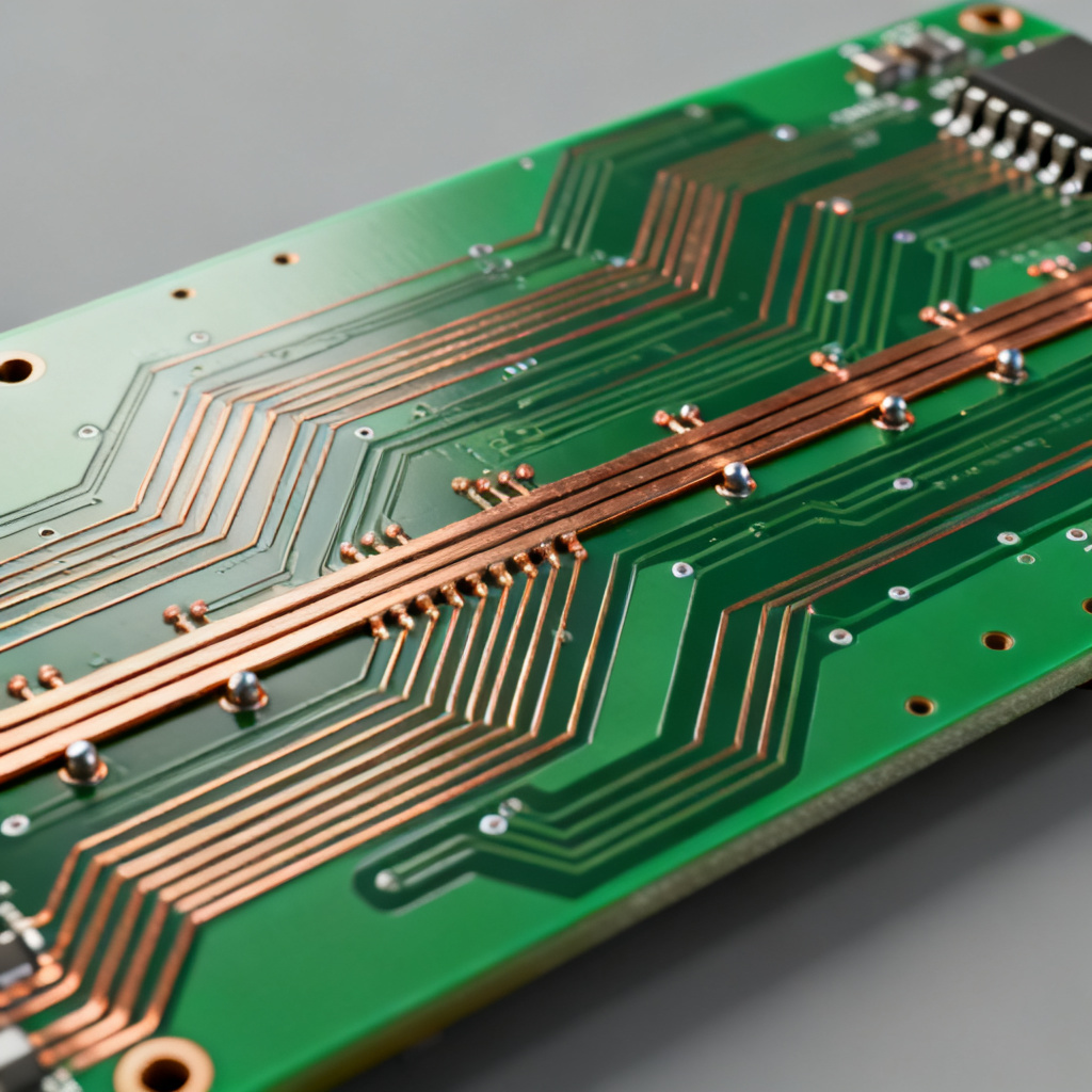
Why Solder Mask Affects Differential Pair Impedance
The Physics Behind the Change
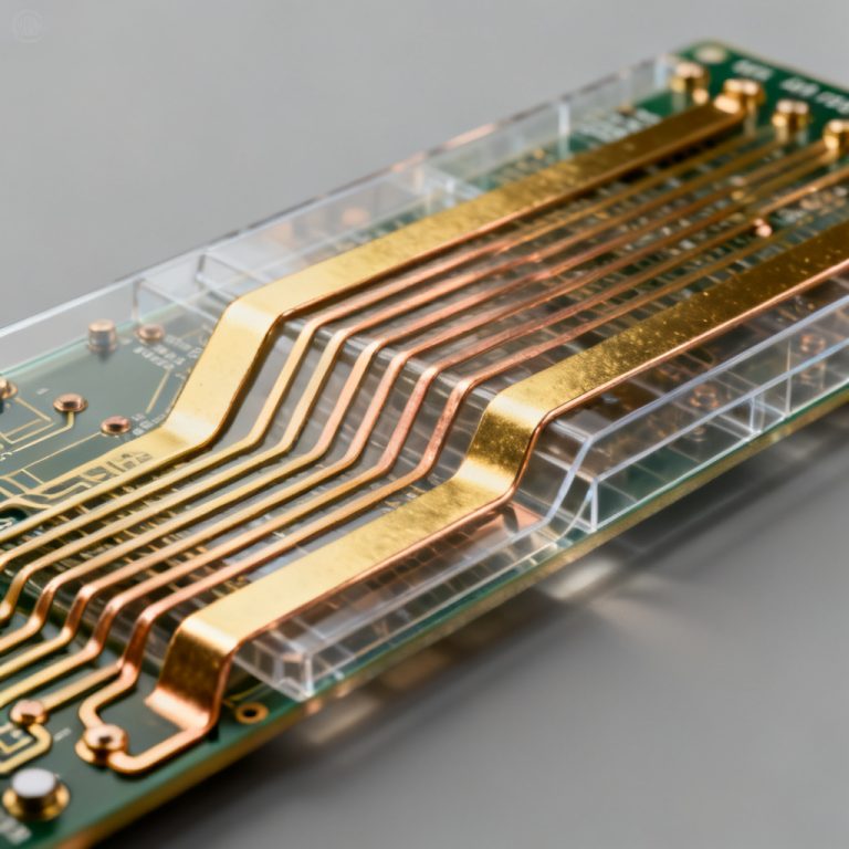
Solder mask is a dielectric material (typically epoxy-based liquid or dry film) applied over copper traces. Its relative permittivity (Dk) usually ranges from 3.3 to 4.5, while the core and prepreg materials have a Dk around 3.5 to 4.2. When solder mask covers a differential pair, it changes the electromagnetic field distribution:
- Increased Capacitance: The solder mask has a higher Dk than air (Dk = 1). Covering the traces with this material increases the capacitance per unit length (C) of the transmission line.
- Reduced Characteristic Impedance: Since characteristic impedance Z0 = sqrt(L/C), an increase in capacitance (C) causes a decrease in impedance.
- Differential Impedance Drop: For differential pairs, the effect is more complex because the solder mask also affects the mutual capacitance between the two traces. The result is a noticeable drop in differential impedance (Zdiff).
Key Factor: Solder Mask Thickness
The amount of impedance change depends heavily on the thickness of the solder mask on the trace edges and top surface. Thinner solder mask (e.g., 0.5 mil) has a smaller effect than thicker mask (e.g., 1.0–1.5 mil). The most critical area is the edge coverage—where the solder mask wraps around the trace corners, it concentrates the electric field, amplifying the capacitive effect.
Solder Mask Dk Variation
Not all solder masks are equal. Standard green solder mask has a Dk of ~3.5–3.8. However, some high-speed-specific solder masks (e.g., Taiyo PSR-4000, Sun Chemical) have lower Dk values (2.8–3.2) to minimize impedance impact. Always check the manufacturer’s datasheet for the exact Dk at your operating frequency (1 GHz to 10 GHz+).
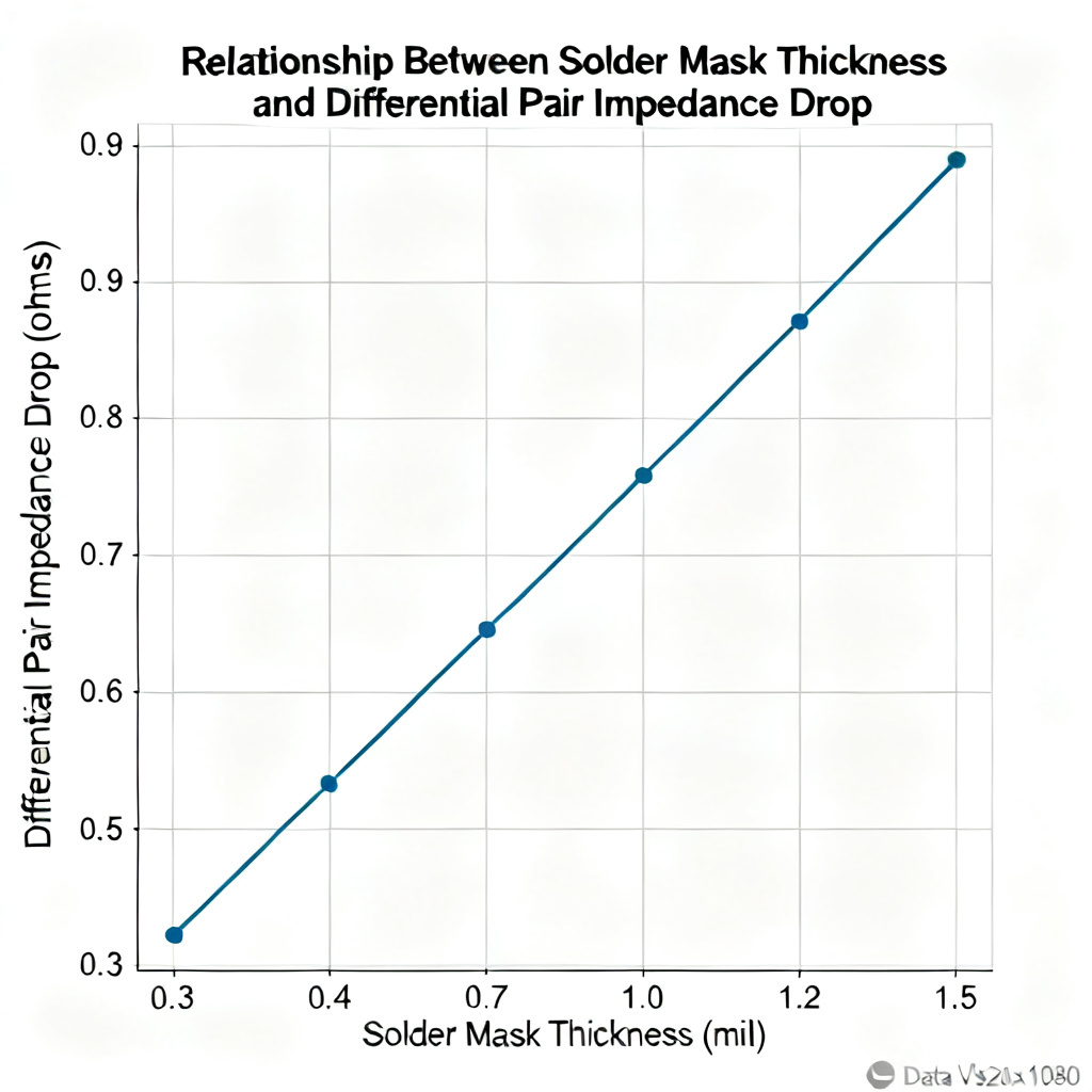
Quantified Impedance Drop Data: How Much Solder Mask Changes Differential Pair Impedance
Real-world measurements and simulations from PCB fabricators and design tool vendors provide specific numbers. The impedance drop is not trivial—it can be 2–10 ohms depending on the geometry.
Typical Impedance Drop Values
- For 100-ohm differential pairs (e.g., USB, Ethernet): Solder mask can reduce Zdiff by 3 to 8 ohms (3% to 8%). Example: A pair designed to be 100 ohms in air may measure 92–97 ohms after solder mask application.
- For 90-ohm differential pairs (e.g., DDR4, HDMI): Drop is typically 2 to 6 ohms.
- For 85-ohm differential pairs (e.g., PCIe Gen4/5): Drop can be 2 to 5 ohms.
Impact of Trace Geometry on Solder Mask Effect
| Trace Width / Spacing | Solder Mask Thickness | Impedance Drop (100Ω target) |
|---|---|---|
| 5 mil / 5 mil (tight coupling) | 0.5 mil | 2–3 ohms |
| 5 mil / 5 mil | 1.0 mil | 4–6 ohms |
| 4 mil / 8 mil (loose coupling) | 0.5 mil | 3–4 ohms |
| 4 mil / 8 mil | 1.0 mil | 6–8 ohms |
Key Insight: Loose-coupled differential pairs (wider spacing) experience a larger percentage drop because the fringing fields extend further laterally, making them more sensitive to the solder mask covering the trace edges.
Frequency Dependence of Solder Mask Effect
The effect is relatively flat from DC to ~5 GHz. Above 10 GHz, the solder mask’s loss tangent (Df) can also introduce additional attenuation, but the impedance drop remains primarily capacitive.
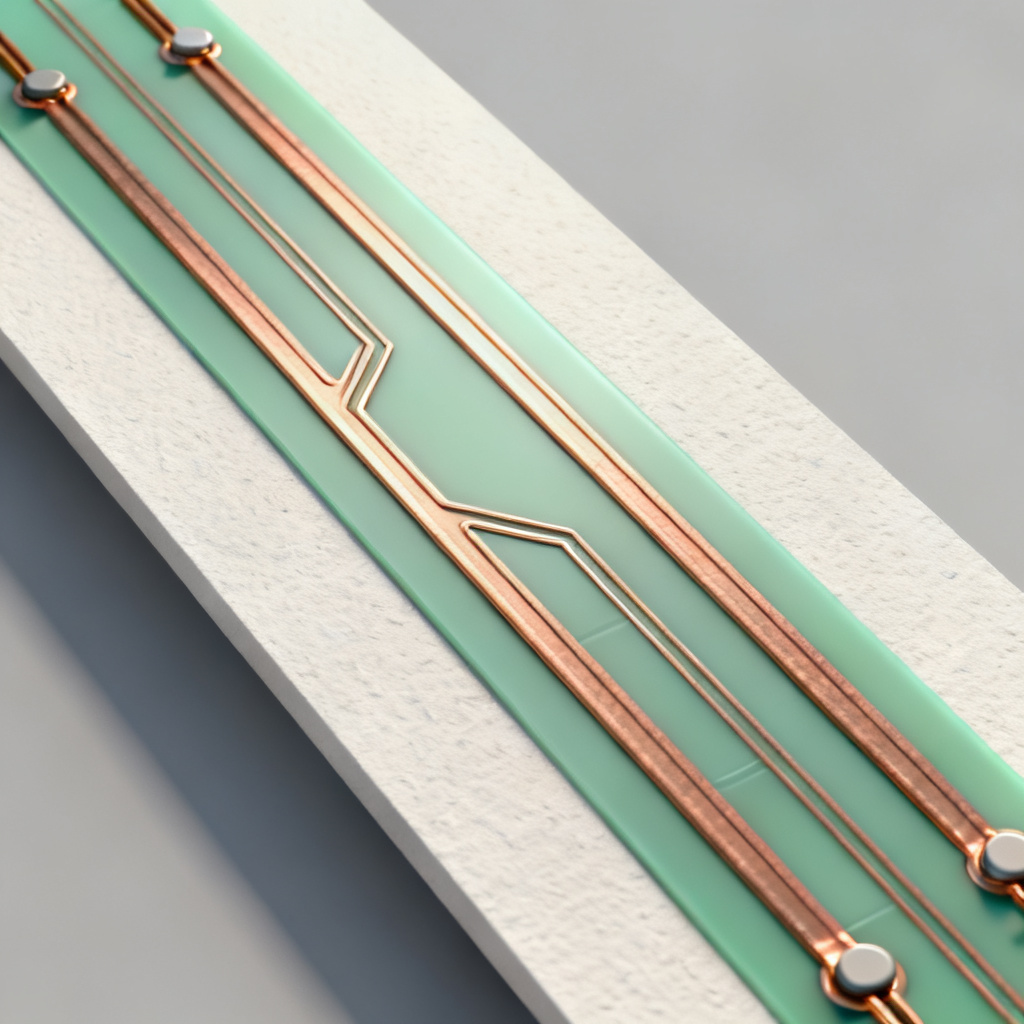
How to Compensate for Solder Mask Impedance Drop in Differential Pairs
When adhering to differential pair routing rules, compensation is essential when your PCB requires tight impedance tolerance (e.g., ±5%). Here are the proven methods used by top-tier PCB fabricators and designers.
Method 1: Adjust Trace Width in the Impedance Calculator
The most common and reliable method is to pre-compensate during the stack-up design stage.
- Step 1: Calculate the required trace width and spacing for your target differential impedance assuming copper is bare (no solder mask).
- Step 2: Add a solder mask layer to your stack-up in your impedance calculator (e.g., Polar Si9000, Saturn PCB Toolkit, Altium Designer’s impedance calculator). Set solder mask thickness to the fabricator’s typical value (usually 0.5–1.0 mil) and Dk to 3.5.
- Step 3: Adjust trace width downward by a small amount (typically 0.5–1.5 mils) to bring the impedance back to the target.
Example: Without solder mask: 100 ohms at 5 mil trace width. With 1.0 mil solder mask: 95 ohms. To restore 100 ohms: Reduce trace width to ~4.2–4.5 mils (depending on coupling).
Caution: Do not change the spacing (gap) between the differential pair, as that would alter the coupling and common-mode impedance. Only adjust trace width.
Method 2: Use a Thinner Solder Mask
If your PCB design allows, request a thinner solder mask from your fabricator. Many high-speed PCB shops offer a “low-profile” solder mask (0.3–0.5 mil) for impedance-critical layers. This reduces the capacitance increase and minimizes the impedance drop to 1–3 ohms.
Method 3: Specify a Low-Dk Solder Mask
For ultra-high-speed designs (e.g., 25 Gbps+), use a solder mask with a Dk of 2.8–3.2. Some fabricators offer “impedance-controlled” solder mask materials. This reduces the capacitive loading by ~20–30% compared to standard green mask.
Method 4: Avoid Solder Mask on Differential Pairs (Selective Mask Removal)
In extreme cases (e.g., RF or millimeter-wave designs), you can specify solder mask removal over critical differential pairs. This is done by adding a “solder mask opening” layer in your Gerber files. However, this exposes copper to oxidation and requires a conformal coating or ENIG finish for protection. It is rarely used for standard high-speed digital designs due to reliability concerns.
Method 5: Account for Solder Mask in the Fabrication Notes
Provide your PCB fabricator with the following information in your fabrication drawing:
- Target differential impedance (e.g., 100 ohms ±5%).
- Solder mask type and thickness (e.g., Taiyo PSR-4000, 0.8 mil).
- Request that they compensate the trace width during their impedance control process.
Most reputable fabricators have their own internal compensation algorithms. If you provide the bare-copper target, they will adjust the trace width to account for their specific solder mask application.
Practical Design Guidelines for Solder Mask and Differential Pair Impedance
Guideline 1: Always Simulate with Solder Mask
Never rely on bare-copper impedance calculations for high-speed designs. Use a 2D field solver (e.g., Polar Si9000, HyperLynx) that models solder mask as a top coating. Many designers mistakenly assume the effect is negligible—it is not.
Guideline 2: Verify with a Coupon
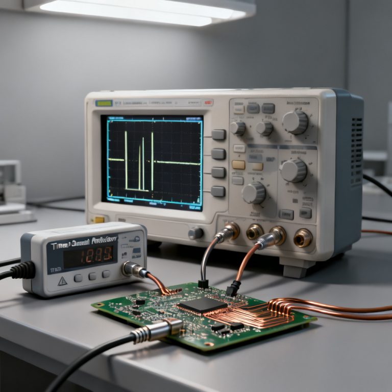
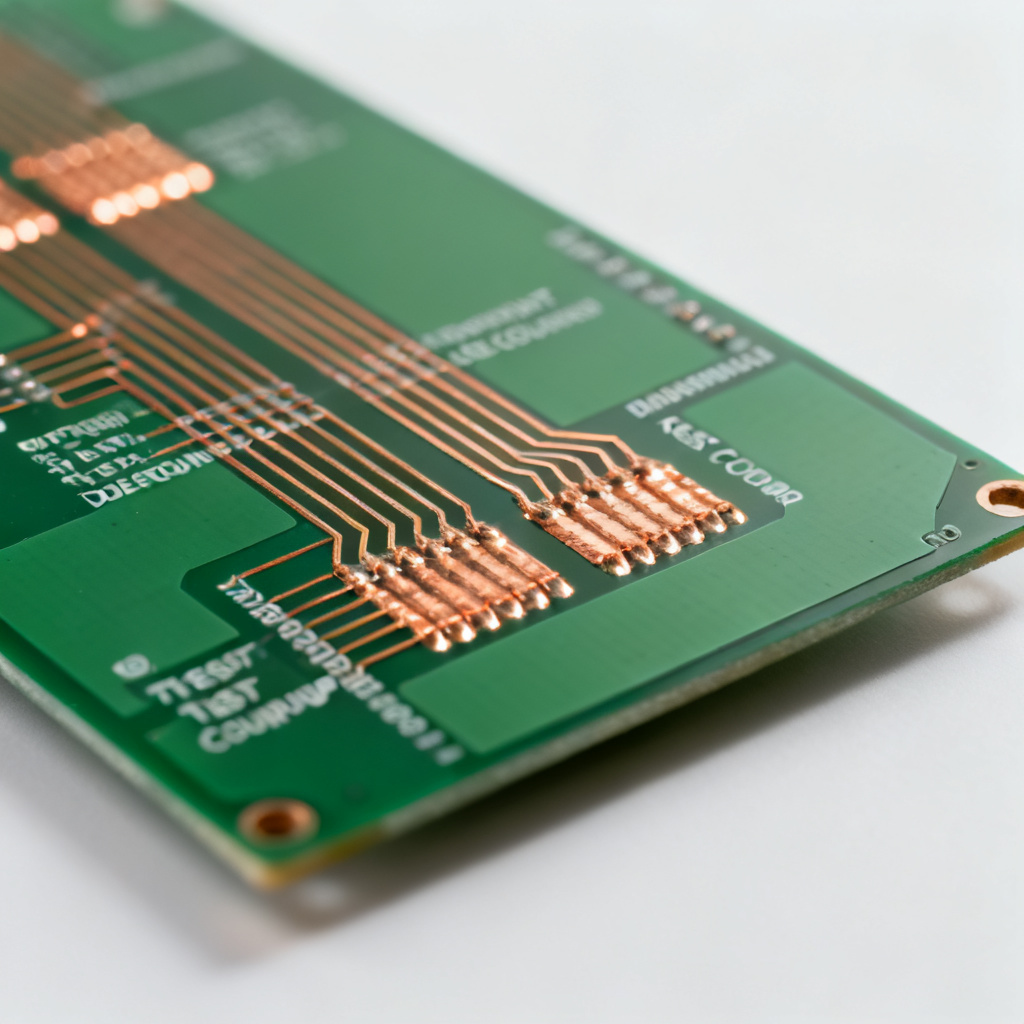
Include an impedance test coupon on your PCB panel. The coupon should have the same trace width, spacing, and solder mask coverage as your actual design. The fabricator will test this coupon to verify the final impedance.
Guideline 3: Watch for Asymmetric Solder Mask Coverage
In differential pairs, if one trace has more solder mask coverage than the other (e.g., near a via or pad), it can cause impedance imbalance and degrade common-mode rejection. Keep solder mask openings symmetrical.
Common Mistake 1: Overcompensating
Reducing trace width too much to compensate for solder mask can increase DC resistance and cause excessive copper loss. A 1.5 mil reduction in trace width can increase resistance by 20–30%. Balance impedance with loss.
Common Mistake 2: Ignoring Solder Mask on Inner Layers
Solder mask is not applied to inner layers in a standard PCB. The effect only occurs on the outer layers (top and bottom). If your differential pair is on an inner layer, solder mask is irrelevant. But if it transitions to an outer layer (e.g., near a connector), the impedance will drop at that transition.
Common Mistake 3: Assuming All Fabricators Use the Same Solder Mask
Different fabricators use different solder mask materials and application methods (liquid vs. dry film). Always ask your specific fabricator for their solder mask Dk and thickness data. Do not rely on generic values.
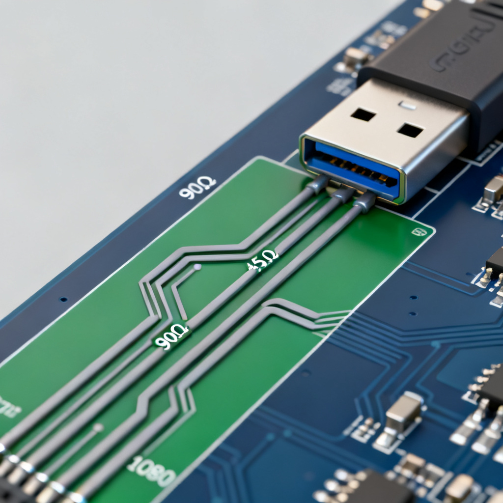
Case Study: Compensating a 100-ohm USB 3.0 Differential Pair
Design Parameters: Stack-up: 4-layer PCB, 1.6 mm total thickness. Target: 100 ohms differential. Outer layer traces: 5 mil width, 5 mil spacing (tight coupling). Solder mask: Standard green, 0.8 mil thick, Dk = 3.6.
Step 1: Bare Copper Calculation Using Polar Si9000 (no solder mask): Trace width = 5.0 mil → Zdiff = 100.2 ohms.
Step 2: With Solder Mask Add 0.8 mil solder mask (Dk = 3.6): Zdiff drops to 94.5 ohms (drop of 5.7 ohms).
Step 3: Compensation Reduce trace width to 4.3 mils (keep spacing at 5 mils): Zdiff returns to 99.8 ohms.
Result: A 0.7 mil reduction in trace width compensates for the solder mask. The DC resistance increases by ~16%, but this is acceptable for USB 3.0 (5 Gbps).
Comparison: Our High-Speed PCB Services vs. Standard Fabricators
| Feature | Our Service | Typical Fabricator |
|---|---|---|
| Solder Mask Dk Data Provided | Yes, per batch | Often generic |
| Impedance Compensation Included | Yes, free | Extra charge |
| Low-Dk Solder Mask Options | Available (Dk 2.8) | Limited |
| Test Coupon Verification | Standard | Optional |
FAQ: Solder Mask and Differential Pair Impedance
How does solder mask affect differential pair impedance?
Solder mask affects differential pair impedance by increasing the capacitance per unit length of the traces, which lowers the characteristic impedance. For differential pairs, this typically results in a drop of 2–8 ohms, depending on solder mask thickness and Dk.
How much should I compensate for solder mask on 100-ohm differential pairs?
For 100-ohm differential pairs, you typically need to compensate by reducing trace width by 0.5–1.5 mils. The exact amount depends on solder mask thickness and coupling; use an impedance calculator with solder mask layer for precision.
Can I ignore solder mask effect on inner layer differential pairs?
Yes, solder mask does not affect inner layer differential pairs because it is only applied to outer layers. However, if the pair transitions to an outer layer, the impedance will change at that point.
What is the best solder mask for high-speed differential pair impedance control?
The best solder mask for high-speed differential pair impedance control is a low-Dk material (Dk 2.8–3.2) with a thin application (0.3–0.5 mil). Examples include Taiyo PSR-4000 and Sun Chemical low-Dk formulations.
Key Terminology for Solder Mask and Differential Pair Impedance
Dielectric Constant (Dk): The relative permittivity of the solder mask material, typically 3.3–4.5 for standard masks. Lower Dk reduces capacitive loading on differential pairs.
Characteristic Impedance (Z0): The impedance of a single-ended transmission line. For differential pairs, Zdiff is the impedance between the two traces.
Fringing Field: The electric field that extends beyond the trace edges. Solder mask on the edges significantly increases capacitance due to this field concentration.
Impedance Test Coupon: A dedicated test structure on the PCB panel used to verify that the differential pair impedance meets the target after manufacturing.
Loss Tangent (Df): A measure of dielectric loss in the solder mask; becomes important above 10 GHz but does not significantly affect impedance magnitude.