Article Summary
High speed pcb prototype lead time directly determines electronics R&D progress, design validation timeline and product launch schedule. For hardware engineers, industrial procurement and project managers, clarifying standard delivery cycles, quick-turn expedited options, hidden influencing factors and production stage breakdown is critical for accurate project scheduling and budget control. This comprehensive high speed pcb prototype lead time guide covers standard lead times by layer count and HDI structure, 24/48/72h urgent service rules, key variables that delay production, full prototype manufacturing time breakdown, pros and cons of rush orders, and practical tips to cut waiting time.
1. How Long Does a High-Speed PCB Prototype Take?
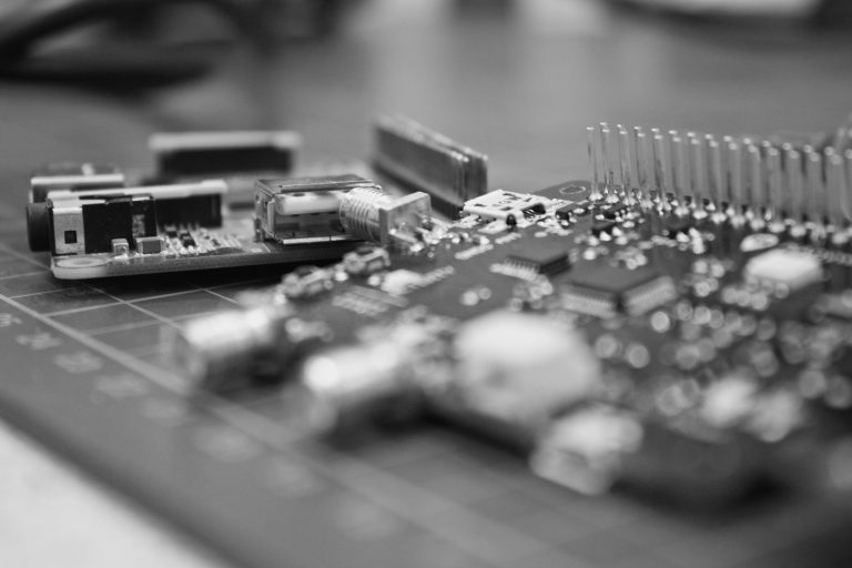
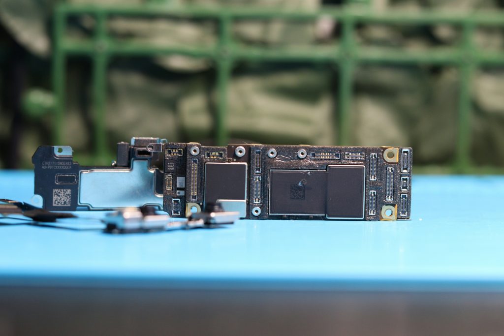
High speed pcb prototype lead time differs greatly from conventional circuit boards due to strict impedance control, low-loss high-frequency materials, precise stackup design and complex lamination processes. All these features make their production lead time longer and more variable than standard PCBs. As detailed in the high-speed PCB cost master page, understanding lead time is as important as understanding cost.
Project delay usually happens when engineering teams fail to reserve enough production time or underestimate extra days needed for HDI structure, special substrates and advanced manufacturing processes. Generally, high speed pcb prototype lead time falls into two main categories: standard regular lead time and quick-turn expedited lead time. The actual turnaround varies based on layer count, stackup type, material grade, testing requirements and factory scheduling status.
This high speed pcb prototype lead time guide organizes industry-standard data from top global PCB manufacturers and technical media, sorting clear lead time tables, hidden delay factors, production phase time allocation, and cost vs speed trade-offs. Whether you are designing 4-layer mainstream high-speed boards, 16-layer high-complexity communication boards or HDI any-layer high-speed designs, you can get accurate time expectations for your prototype order.
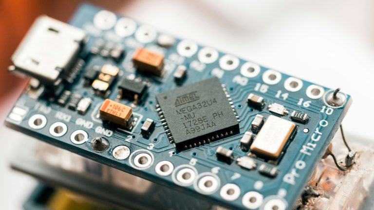
2. Standard High-Speed PCB Prototype Lead Times by Layer & Structure
Standard lead time refers to normal production scheduling without priority rush arrangement, calculated in working days. It is the most cost-effective option for routine design verification. For PCB Manufacturing, standard lead times are the baseline.
| PCB Layer Count | Standard Lead Time (Working Days) | Professional Description |
|---|---|---|
| 4–6 Layers | 5–7 Days | Standard FR4 high-speed substrate, basic impedance control |
| 8–10 Layers | 6–8 Days | Moderate routing density, strict inner-layer stackup |
| 12–16 Layers | 8–10 Days | High-layer board with precise impedance tolerance |
| 18 Layers & Above | 10–14 Days | Ultra-high-layer requiring multiple lamination, high-precision alignment |
HDI Structure Extra Lead Time:
- HDI (1+N+1): +2–4 working days
- Any-layer HDI: +5–8 working days
Most 4–8 layer regular high-speed projects fit perfectly within the 5–7 day standard cycle. Understanding high speed pcb prototype lead time for HDI structures helps you reserve extra time in your project timeline.
3. Quick-Turn / Expedited High-Speed PCB Prototype Lead Times
When facing tight R&D deadlines, emergency equipment repair, urgent design bug verification and fixed market launch windows, quick-turn expedited service becomes necessary. For quick turn pcb service, similar lead time options are available.
| Service Level | Guaranteed Lead Time | Maximum Layer Limit | Cost Premium vs Standard |
|---|---|---|---|
| 24-Hour Rush | 24 Hours | ≤4 Layers | +100–200% |
| 48-Hour Rush | 48 Hours | 6–8 Layers | +75–150% |
| 72-Hour Rush | 72 Hours | 8–10 Layers | +50–100% |
| 5-Day Expedited | 5 Working Days | ≤12 Layers | +30–60% |
Important notes for high speed pcb prototype lead time:
- 24h ultra-rush only supports simple low-layer high-speed boards
- Expedited lead time covers production only, excluding material procurement and file revision time
- For 12-layer and above high-speed prototypes beyond 72h capacity, the 5-day expedited option balances speed and budget well
For high speed PCB prototype cost, expedited services add significant premiums.
4. Key Factors That Affect High-Speed PCB Prototype Lead Time
Even with confirmed standard or expedited orders, multiple technical and supply-side factors can unexpectedly extend high speed pcb prototype lead time. For High-Speed PCB Material, material availability is a key factor.
| Influencing Factor | Potential Delay | Detailed Explanation |
|---|---|---|
| Special Material Supply | +3–10 Days | High-frequency substrates like Rogers rely on imported inventory |
| Process Complexity | +2–5 Days | Back-drilling, hybrid lamination require extra production steps |
| Custom High-Speed Testing | +1–2 Days | Full TDR impedance test, high-frequency inspection take extra time |
| Post-DFM Design Modification | Reset Full Cycle | Design revision restarts CAM and production flow completely |
| Factory Peak Scheduling | Uncertain Delay | Industry busy seasons squeeze prototype capacity |
Among all factors, special material supply and DFM design modification are the top two causes of unexpected delays in high speed pcb prototype lead time. Engineers should complete self-DFM checking and confirm material stock before submitting files. For pcb cost factors, similar preparation helps avoid cost overruns.
5. High-Speed PCB Prototype Lead Time Breakdown by Production Stage
The entire prototype cycle can be split into standardized phases, letting you clearly see where time is consumed and which stage can be optimized for high speed pcb prototype lead time.
| Production Stage | Time Consumption | Percentage of Total Lead Time |
|---|---|---|
| DFM Check & CAM Engineering | 4–8 Hours | 5–10% |
| Raw Material Preparation & Cutting | 4–8 Hours | 5–10% |
| Core PCB Manufacturing | 3–5 Days | 60–70% |
| Electrical & Quality Testing | 4–8 Hours | 5–10% |
| Final Inspection & Shipment | 4–8 Hours | 5–10% |
Understanding this breakdown helps you target the right stages for high speed pcb prototype lead time reduction. The core manufacturing stage dominates the whole cycle, covering inner layer etching, lamination, drilling, plating, solder mask and silkscreen.
6. Quick-Turn Prototype Trade-Offs: Benefits & Drawbacks
Quick-turn service brings obvious time advantages, but it also has unavoidable trade-offs in cost, design flexibility and testing completeness when considering high speed pcb prototype lead time.
Core Benefits:
- Accelerate design validation and hardware iteration speed
- Meet rigid product launch deadlines and seize market opportunities
- Support on-site emergency equipment repair
Key Drawbacks:
- Significant cost increase with 30% to 200% extra service fee
- Factories usually require design freeze after DFM confirmation, no further revisions
- Ultra-fast 24–48h orders may skip partial professional high-speed testing items
Engineers and procurement teams need to balance time urgency, budget and testing completeness before choosing rush production. For high speed PCB mass production cost, similar trade-offs apply.
7. Practical Tips to Shorten High-Speed PCB Prototype Lead Time
You do not have to rely entirely on expensive expedited services to save time. With standardized preparation and reasonable planning, you can effectively shorten high speed pcb prototype lead time under standard production arrangements.
- Reserve special materials in advance – Communicate with PCB manufacturers early to confirm stock of high-frequency substrates, avoiding long procurement delays
- Submit complete and standardized design files one time – Provide finished Gerber files, stackup details, impedance requirements to avoid repeated confirmation
- Adopt standard stackup and regular specifications – Use industry common layer structures, standard hole sizes to reduce custom process difficulty
- Avoid factory peak seasons – Arrange prototype orders in non-peak periods to escape production congestion
- Complete self-DFM inspection before submission – Fix trace spacing, via location and stackup problems in advance to prevent cycle reset
8. Key Takeaways
- Standard high speed pcb prototype lead time ranges from 5–7 working days for 4–6 layers to 10–14 days for 18 layers and above; HDI adds 2–8 extra days
- Quick-turn options cover 24h/48h/72h ultra-rush for low to medium layers and 5-day expedited service for up to 12 layers, with clear cost premiums
- Material supply, complex processes, custom testing, DFM revisions and factory scheduling are the main factors causing delivery delay
- Core manufacturing occupies 60–70% of the total cycle; pre-production DFM and material preparation are critical for on-time delivery
- Expedited service saves time but comes with higher cost, design freeze limits and possible testing compromises
For a complete understanding of all cost and lead time topics, return to the high-speed PCB cost master page.
9. FAQ About High-Speed PCB Prototype Lead Time
Q1: How long does a 4-layer high-speed PCB prototype take normally?
Standard 5–7 working days; 24-hour expedited service is available with 100–200% cost premium. This is the baseline for high speed pcb prototype lead time planning.
Q2: Will HDI high-speed PCB take longer than regular multilayer boards?
Yes, 1+N+1 HDI adds 2–4 days, any-layer HDI adds 5–8 extra working days due to laser via and multiple lamination.
Q3: Why does high-speed PCB lead time longer than ordinary PCB?
Strict impedance control, low-loss high-frequency materials, complex stackup and extra TDR testing all increase production steps and inspection time.
Q4: Can I modify my design after DFM review?
Design changes after DFM will reset the entire production cycle and cause obvious delay; it is recommended to finish all revisions before file submission.
Q5: Is expedited lead time including shipping time?
No, quick-turn time only covers factory production; shipping time is calculated separately based on your shipping method and destination.
10. Get Fast & Reliable High-Speed PCB Prototype Quote
Need accurate lead time confirmation and competitive pricing for your high-speed PCB prototype? We provide one-stop high-speed PCB manufacturing service covering 4-layer to 18+ layer boards, HDI/any-layer HDI structure, high-frequency materials and professional TDR impedance testing.
We offer both standard cost-effective delivery and flexible 24–72 hour quick-turn options, with transparent pricing, full DFM support and real-time order progress tracking. Our team can help you optimize high speed pcb prototype lead time without unexpected delays.
Submit your Gerber files and design requirements now to get an instant official quote and confirmed lead time for your high-speed PCB prototype project.