Spectrum analyzer for periodic jitter is a critical tool in high-speed PCB design, where periodic jitter itself is a major signal integrity challenge. This guide explains how to use a spectrum analyzer to detect, measure, and mitigate periodic jitter in high-speed PCB systems, providing engineers with a reliable frequency-domain approach for identifying noise sources such .
Understanding Periodic Jitter in High Speed PCB
What is Periodic Jitter in High Speed PCB?
Periodic jitter in high speed PCB is a deterministic jitter component that repeats at a fixed frequency. Typical sources include clock harmonics, switching power supply ripple, and crosstalk from adjacent traces. In the frequency domain, periodic jitter in high speed PCB appears as discrete sidebands around the carrier frequency.
Spectrum Analyzer vs Oscilloscope for Periodic Jitter in High Speed PCB
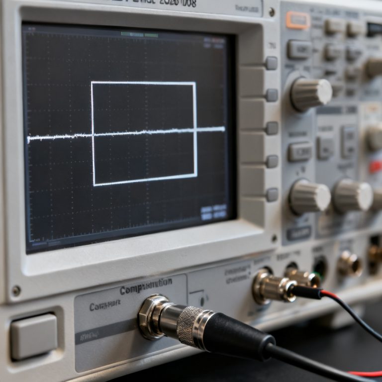
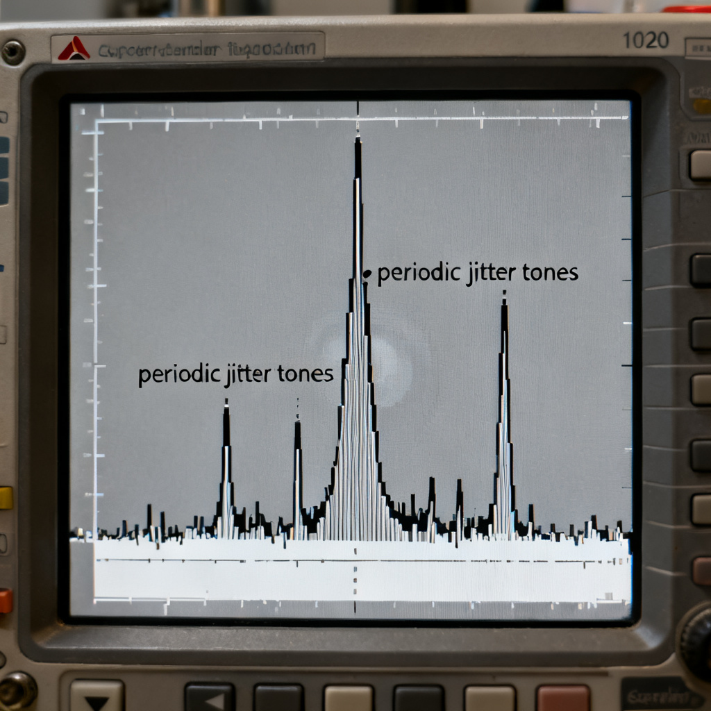
While oscilloscopes measure total jitter, a spectrum analyzer offers higher dynamic range for detecting low-amplitude periodic jitter in high speed PCB. It provides frequency selectivity to isolate specific jitter tones and enables modulation analysis for identifying the exact jitter source frequency.
Equipment Setup for Periodic Jitter in High Speed PCB
Choosing the Right Spectrum Analyzer for Periodic Jitter in High Speed PCB
For periodic jitter in high speed PCB analysis, select a spectrum analyzer with a frequency range at least 3× the data rate, low phase noise floor (e.g., < -120 dBc/Hz at 10 kHz offset), and resolution bandwidth as low as 1 Hz. A real-time spectrum analyzer is recommended for capturing transient periodic jitter in high speed PCB events.
Probing and Signal Conditioning for Periodic Jitter in High Speed PCB
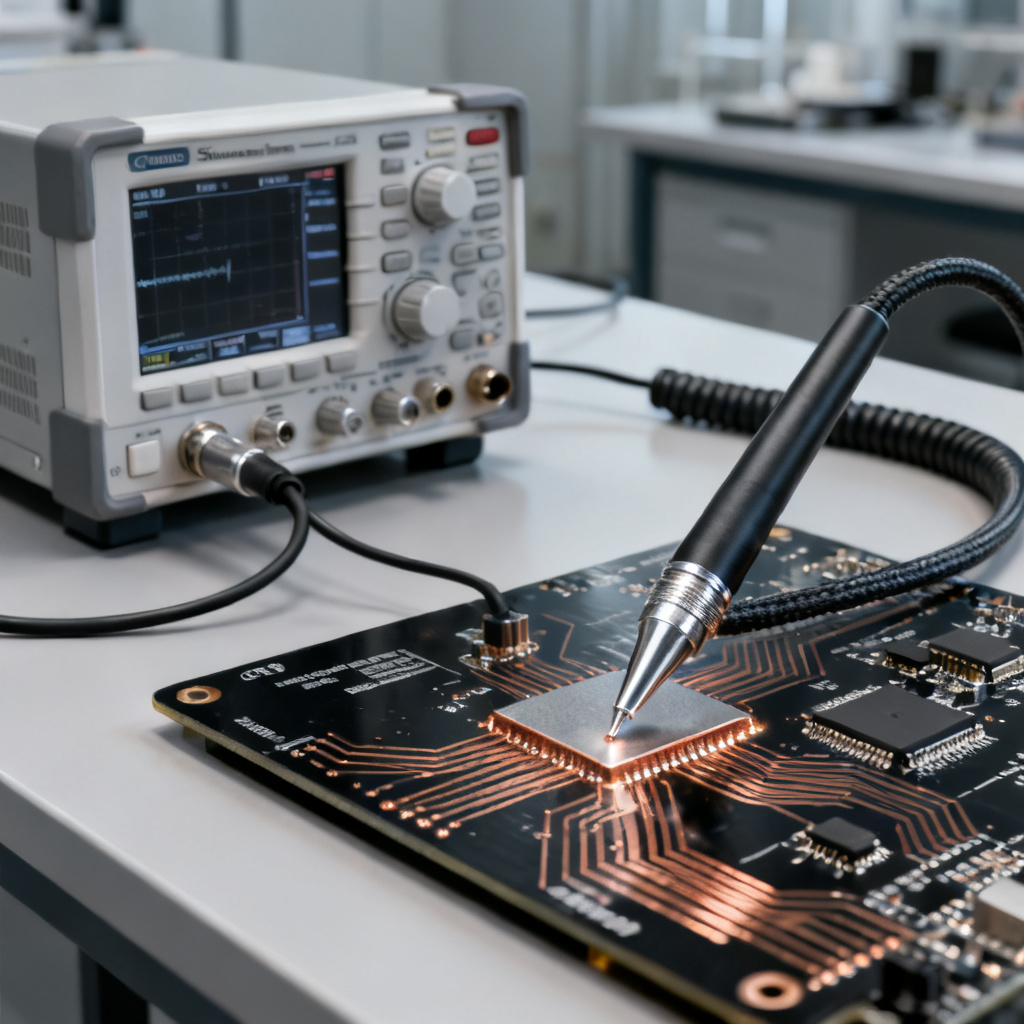
Use a high-impedance active probe for low-frequency periodic jitter in high speed PCB (< 1 GHz). For high-frequency PJ (> 1 GHz), use a broadband balun or differential probe. Add a pre-amplifier if the signal amplitude is below the analyzer’s noise floor. Probe at the receiver end of the PCB trace, avoiding power supply pins or noisy vias.
Analyzer Settings for Periodic Jitter in High Speed PCB
Set the center frequency to the carrier, span to 10× the expected PJ frequency, RBW to 1% of span, VBW to 1× RBW, and use peak detector for sideband identification. For fine periodic jitter in high speed PCB detection, reduce RBW to 10 kHz–100 kHz.
Measurement Methodology for Periodic Jitter in High Speed PCB
Step 1: Baseline Measurement for Periodic Jitter in High Speed PCB
Capture the carrier spectrum with a wide span (e.g., 10× data rate). Identify any spurious emissions or harmonics. The carrier should be at least 20 dB above any sideband to avoid masking periodic jitter in high speed PCB.
Step 2: Identify Sidebands from Periodic Jitter in High Speed PCB
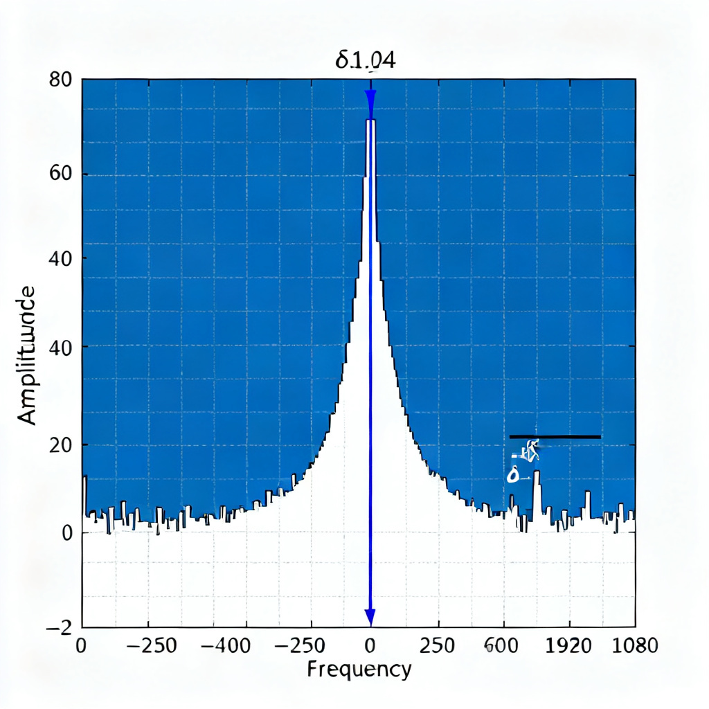
Set the analyzer to a narrow span (e.g., ±10 MHz around carrier) with low RBW (e.g., 10 kHz). Look for discrete tones offset from the carrier by ±f_PJ. Record the amplitude of each sideband in dBc relative to carrier. Use the marker delta function for direct measurement.
Step 3: Convert Sideband Amplitude to Jitter for Periodic Jitter in High Speed PCB
The relationship between sideband amplitude (A_sideband, in dBc) and peak-to-peak jitter (J_pp, in UI) is: J_pp = (2 × 10^(A_sideband/20)) / π. For example, A_sideband = -60 dBc yields J_pp = 0.000637 UI. For a 2.5 Gbps signal (400 ps UI), this equals 0.255 ps of periodic jitter in high speed PCB.
Step 4: Identify the Source of Periodic Jitter in High Speed PCB
Use the PJ frequency to trace the source: if f_PJ matches a clock frequency, check clock distribution; if it matches power supply ripple, use a near-field probe; if it is a sub-harmonic of the data rate, check for crosstalk. Use spectrogram mode to visualize periodic jitter in high speed PCB over time.
Advanced Techniques for Periodic Jitter in High Speed PCB
Multiple Periodic Jitter Tones in High Speed PCB
Real-world PCBs often have multiple PJ sources. Use a wide span (e.g., 100 MHz) with low RBW (10 kHz) to record all sideband frequencies and amplitudes. Use the phase noise plot to see the overall jitter profile. Sum the jitter contributions using root-sum-square for uncorrelated sources.
Periodic Jitter from Data-Dependent Effects in High Speed PCB
Data-dependent jitter (DDJ) often has a periodic component due to pattern repetition. Use a vector signal analyzer with pattern-sync capability. Trigger on the pattern repetition rate and look for sidebands at multiples of the pattern rate. For PRBS7 (127 bits) at 2.5 Gbps, sidebands at 19.7 MHz indicate DDJ.
Phase Noise Integration for Periodic Jitter in High Speed PCB
Switch to phase noise measurement mode and set integration bandwidth from 10 Hz to 10 MHz. The analyzer outputs RMS jitter in seconds. This method assumes all noise is phase noise; use for relative comparisons of periodic jitter in high speed PCB.
Practical Tips for Periodic Jitter in High Speed PCB
Common Pitfalls in Periodic Jitter in High Speed PCB Measurement
| Pitfall | Consequence | Solution |
|---|---|---|
| Insufficient RBW | Misses close-in sidebands | Use RBW < 1% of expected PJ frequency |
| Probe loading | Alters jitter behavior | Use active probe with < 0.5 pF capacitance |
| Ground loop noise | Adds false PJ tones | Use isolated ground connection |
| Carrier compression | Non-linear sidebands | Keep carrier power < -20 dBm at analyzer input |
| Aliasing from under-sampling | False sidebands | Use real-time bandwidth > 2× PJ frequency |
Correlating Results for Periodic Jitter in High Speed PCB
Validate your findings by measuring total jitter with an oscilloscope. Compare the PJ amplitude from the spectrum analyzer with the oscilloscope’s jitter decomposition. If they match within 20%, your measurement of periodic jitter in high speed PCB is reliable.
Spectrum Analyzer vs Phase Noise Analyzer for Periodic Jitter in High Speed PCB
A spectrum analyzer is best for identifying specific PJ tones and their frequencies, making it cost-effective for general lab use. A phase noise analyzer is better for ultra-low jitter measurements (< 100 fs RMS). Start with a spectrum analyzer for periodic jitter in high speed PCB debugging.
Case Study: Debugging Periodic Jitter in High Speed PCB
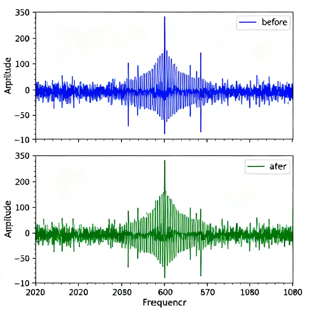
A 10 Gbps PCB design showed intermittent bit errors. Using a spectrum analyzer set to center frequency = 10 GHz, span = 100 MHz, RBW = 100 kHz, two sidebands were identified: at ±1 MHz (-55 dBc) and ±10 MHz (-70 dBc). Conversion yielded 0.28 ps and 0.063 ps of periodic jitter in high speed PCB, respectively. The 1 MHz tone matched the buck converter switching frequency; the 10 MHz tone matched the PLL reference clock. Adding a ferrite bead and notch filter reduced PJ to 0.1 ps.
Frequently Asked Questions about Periodic Jitter in High Speed PCB
What is the main cause of periodic jitter in high speed PCB?
Common causes include clock harmonics, switching power supply ripple, crosstalk from adjacent traces, and EMI coupling. These sources create discrete frequency components that appear as sidebands around the carrier in spectrum analyzer measurements.
How do I measure periodic jitter in high speed PCB with a spectrum analyzer?
Set the analyzer to the carrier frequency, use a narrow span (e.g., ±10 MHz), low RBW (e.g., 10 kHz), and look for discrete sidebands. Convert the sideband amplitude to jitter using the formula J_pp = (2 × 10^(A_sideband/20)) / π.
Can a spectrum analyzer replace an oscilloscope for periodic jitter in high speed PCB?
No. A spectrum analyzer excels at identifying the frequency and amplitude of periodic jitter, but it cannot measure total jitter or random jitter directly. Use both tools together for comprehensive signal integrity analysis.
What RBW setting is best for detecting periodic jitter in high speed PCB?
Start with RBW set to 1% of the span. For fine detection of close-in sidebands, reduce RBW to 10 kHz–100 kHz. Lower RBW improves frequency resolution but increases sweep time.
How do I reduce periodic jitter in high speed PCB designs?
Add ferrite beads to power rails, use notch filters on PLL inputs, increase trace spacing to reduce crosstalk, and improve power supply decoupling. Validate changes with a spectrum analyzer to confirm PJ reduction.
Glossary of Key Terms for Periodic Jitter in High Speed PCB
- Periodic jitter (PJ): A deterministic jitter component that repeats at a fixed frequency, often caused by clock harmonics or power supply noise.
- Sideband: Discrete frequency components offset from the carrier, indicating the presence and frequency of periodic jitter.
- Resolution bandwidth (RBW): The frequency resolution of a spectrum analyzer; lower RBW improves the ability to distinguish close-in sidebands.
- Phase noise: Random fluctuations in the phase of a signal; integrated phase noise can be converted to jitter.
- Data-dependent jitter (DDJ): Jitter that correlates with the data pattern, often having periodic components due to pattern repetition.