Article Abstract
Driven by AI, cloud computing and enterprise big data expansion, modern data centers are rapidly upgrading to 400G, 800G and ultra-high-speed interconnection architectures. As the core physical carrier of signal transmission and power distribution, data center PCB design determines system performance, stability and long-term reliability. This all-in-one pillar guide systematically explains data center PCB classification, key design parameters, high-speed serial routing rules, backplane design challenges, low-loss material grading selection and professional design checklist. Written for hardware engineers, PCB designers and international procurement buyers, it balances professional technical depth with easy-to-understand logic, following industry standard specifications and Google SEO structure, serving as a permanent reference page for data center PCB design and manufacturing.
Overview of Data Center PCB Design
The booming development of artificial intelligence, cloud computing and large-scale data storage has reshaped modern data center bandwidth demands. Network traffic continues to explode, pushing rates from 25Gbps to 100G, 400G and 800G. AI server PCB design shares many principles with data center applications.
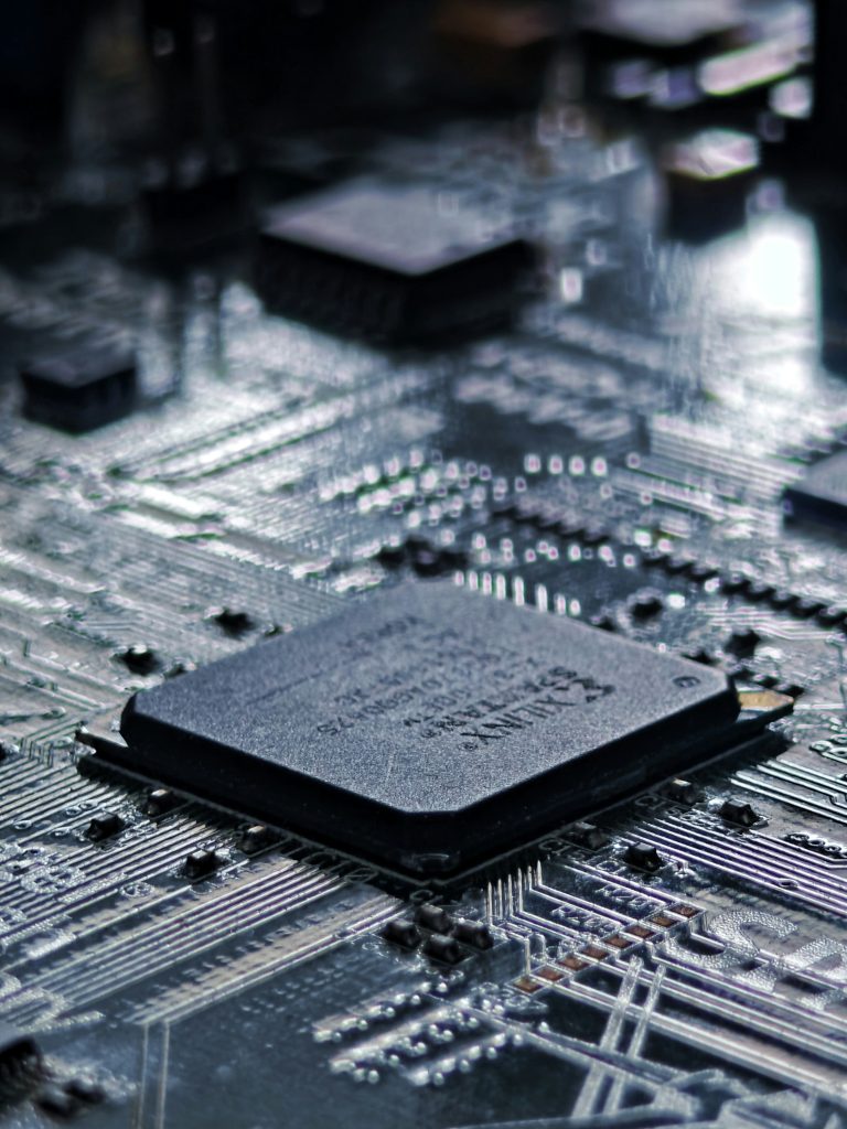
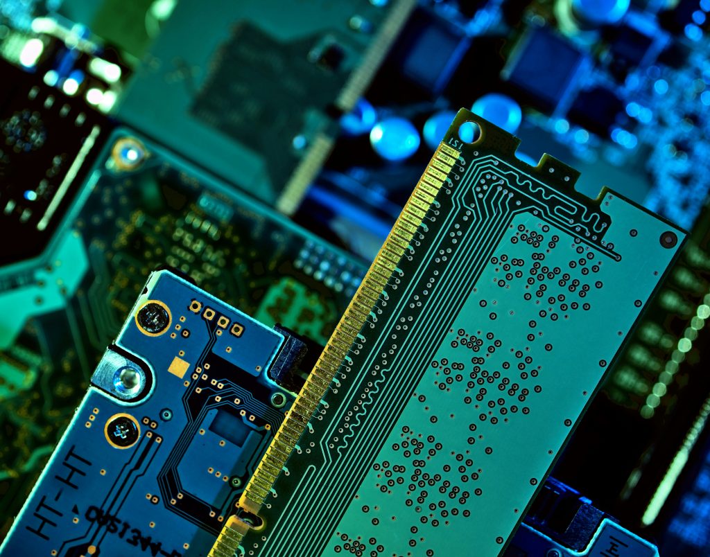
PCB acts as the fundamental hardware carrier for signal interconnection and power delivery in data center facilities. Unlike consumer-grade boards, data center PCB design demands ultra-high transmission speed, high component density, and long-term reliability.
These characteristics set strict requirements on layer stackup, high-frequency substrate selection, impedance control, and crosstalk suppression. Every data center PCB design must balance signal integrity, power integrity, thermal dissipation and manufacturability.
Main Types of Data Center PCBs & Application Scenarios
Understanding the four main PCB types is essential for effective data center PCB design. Each category has unique design difficulty and stackup configuration.
。Core Router PCB。Server Motherboard。Storage Backplane
| PCB Type | Core Function | Typical Rate & Capacity | Typical Layer Count |
|---|---|---|---|
| Network Switch PCB | Mass data packet forwarding | 12.8T – 51.2T switching capacity | 16–28 layers |
| Backbone network transmission | 400G / 800G port speed | 16–24 layers | |
| CPU, memory and accelerator interconnection | PCIe 5.0 / PCIe 6.0 | 12–20 layers | |
| HDD / SSD array docking | 12G / 24G SAS, PCIe channels | 10–20 layers |
Switch and router PCBs require multi-layer dense stacking for massive high-speed differential pairs. Server motherboards focus on CPU power stability. Storage backplanes face long-channel transmission challenges. A complete data center PCB design must address each type’s unique requirements.
Core Design Parameters for Data Center PCB Design
Standardized parameter definition is the foundation of qualified data center PCB design. Different equipment adopts differentiated configurations.
。Board Thickness。Material Grade。Copper Thickness。Surface Treatment
| Design Parameter | Switch & Router PCB | Server Motherboard PCB |
|---|---|---|
| Layer Count | 16–28 layers | 12–20 layers |
| 2.0–3.2 mm | 1.6–2.4 mm | |
| Low-loss / Ultra-low-loss | Low-loss | |
| 1–2 oz | 1 oz | |
| ENIG | ENIG |
High-layer and thicker board design enhances structural rigidity. ENIG surface treatment provides excellent flatness and high-frequency stability, perfectly matching long-term data center PCB design requirements.
High-Speed Serial Interface Routing Standards
Reasonable differential pair routing directly controls signal attenuation and bit error rate. PCIe PCB Design and Impedance Matching provide complementary high-speed routing guidelines.
。25G Ethernet。50G Ethernet。100G Ethernet。PCIe 5.0
| Interface Standard | Line Rate | Differential Impedance | Intra-Pair Mismatch |
|---|---|---|---|
| 25.78Gbps | 100Ω | ≤3 mil | |
| 53.125Gbps PAM4 | 100Ω | ≤2 mil | |
| 106.25Gbps PAM4 | 100Ω | ≤1–2 mil | |
| 32GT/s | 100Ω | ≤2–3 mil |
All mainstream interfaces adopt unified 100Ω differential impedance. As PAM4 rates increase, the signal eye margin narrows, requiring stricter length matching precision. High-speed differential pairs in any data center PCB design must maintain consistent line width and spacing.
Critical Backplane Design Considerations & Solutions
Backplane PCB is often the weakest link in data center PCB design, featuring long channels, dense vias and complex stacking. PCB Manufacturing covers backdrilling and via optimization.
。Excessive insertion loss。Via stub interference。Inter-pair crosstalk。Incomplete return path
| Design Challenge | Professional Solution |
|---|---|
| Adopt ultra-low-loss substrates; optimize routing path | |
| Apply backdrilling to remove redundant via stubs | |
| Increase spacing; add ground guard traces | |
| Arrange dense stitching vias for continuous ground return |
Backdrilling is indispensable for high-speed data center PCB design, effectively eliminating stub resonance and extra loss. Complete reference planes stabilize impedance and shield EMI interference.
Low-Loss Material Selection by Data Rate
PCB substrate material is the decisive factor of high-frequency signal loss. High-Speed PCB Material provides detailed Dk/Df values for common laminates.
。≤10Gbps。10–28Gbps。28–56Gbps。56–112Gbps
| Signal Rate Range | Recommended Material Grade | Application Scenarios |
|---|---|---|
| Medium-Low Loss | Management signals, low-speed ports | |
| Low-Loss | 25G Ethernet ports, server peripheral | |
| Ultra-Low-Loss | 50G Ethernet, high-end accelerator | |
| Ultra-Low-Loss | 100G/400G PAM4, core router channels |
Low-loss and ultra-low-loss substrates maintain stable low Dk and Df values under high frequency. For 50G and above channels, ultra-low-loss materials are mandatory. Proper material selection is a critical step in data center PCB design.
Professional Data Center PCB Design Checklist
This standardized checklist helps ensure design compliance and long-term stable operation for any data center PCB design project:
| ✅ | Item |
|---|---|
| ✅ | All high-speed differential pairs and backplane connector vias implement backdrilling |
| ✅ | Control high-speed line impedance tolerance within ±10% |
| ✅ | Select substrate materials strictly according to rate grading |
| ✅ | Limit via transitions per high-speed channel to ≤2 times |
| ✅ | Keep ground and power reference planes complete and continuous |
| ✅ | Reserve sufficient spacing between differential pairs to suppress crosstalk |
| ✅ | Verify layer count, board thickness, copper weight and surface treatment |
Key Takeaways for Data Center PCB Design
- Data centers are evolving toward 400G and 800G interconnection, raising requirements for data center PCB design.
- Switches, routers, server motherboards and storage backplanes each have independent design parameters.
- Backplane design remains the bottleneck of overall signal integrity due to long channels and dense vias.
- Substrate loss grade directly determines maximum supportable transmission rate.
- Professional data center PCB design must combine signal integrity simulation, industrial standards and process capability.
FAQ About Data Center PCB Design
Q1: What is the standard layer count for data center PCBs?
Switches and routers: 16–28 layers; server motherboards: 12–20 layers; storage backplanes: 10–20 layers. This is a fundamental data center PCB design decision.
Q2: Why is ultra-low-loss material mandatory for 100G/400G designs?
100G+ PAM4 signals have smaller eye opening margin; ultra-low-loss materials reduce dielectric insertion loss and ensure signal quality.
Q3: Is backdrilling necessary for all data center PCBs?
Mandatory for backplanes and high-speed switch/router boards; low-speed layers can omit backdrilling to control cost.
Q4: What impedance is used for data center high-speed differential pairs?
100Ω differential impedance is the unified industry standard for 25G–100G Ethernet and PCIe channels.
Q5: What surface treatment is best for data center PCBs?
ENIG is most widely used for flatness, high-frequency stability, oxidation resistance and long-term reliability.
For a complete understanding of all high-speed PCB application scenarios, return to the high speed PCB applications master page.
Custom Data Center PCB Design & Manufacturing Support
We provide one-stop professional services for data center PCB design: high-layer stackup, low-loss material selection, backdrilling processing, prototype proofing and mass production. We support 100G/400G high-speed channel customization and full reliability testing.
Send your project specifications, rate requirements and layer demands. Our engineering team will reply with a tailored technical solution and competitive quote.
© 2026 HighSpeedPCBs –