Abstract
Small batch PCB production bridges the critical gap between prototype validation and full-scale mass production. After a prototype proves functional, engineers need to verify manufacturability, test market response, and build early inventory – all without committing to thousands of pieces. This is where small batch production (10–250 pieces) becomes indispensable.
This pillar guide integrates three authoritative sources:
- JLCPCB – NRE cost analysis, component sourcing, and DFM optimization
- NextPCB – three-stage comparison, best practices, and challenge solutions
- PCBCart – decision framework, prototype vs production capability tables
The result is a complete, engineer-approved reference for small batch PCB production – suitable for hardware developers, procurement buyers, and industrial project managers.
📖 Table of Contents:
- 3. What Is Small Batch PCB Production?
- 4. Quantity Options & Application Scenarios
- 5. Prototype vs Small Batch vs Mass Production
- 6. Core Advantages of Small Batch Production
- 7. Technical Specifications & Manufacturing Capabilities
- 8. Cost Structure & NRE Analysis
- 9. Complete Production Workflow
- 10. Common Challenges & Engineering Solutions
- 11. How to Choose the Right Small Batch Manufacturer
- 12. DFM Optimization & Best Practices
- 13. Complete Small Batch Production Checklist
- 14. Key Takeaways
- 15. Frequently Asked Questions (FAQ)
- 16. Get Your Small Batch Production Quote
What Is Small Batch PCB Production?
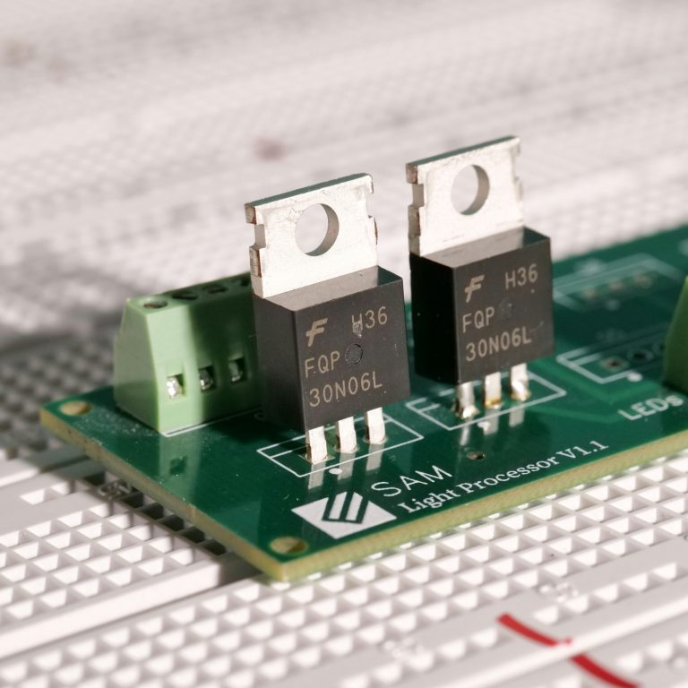
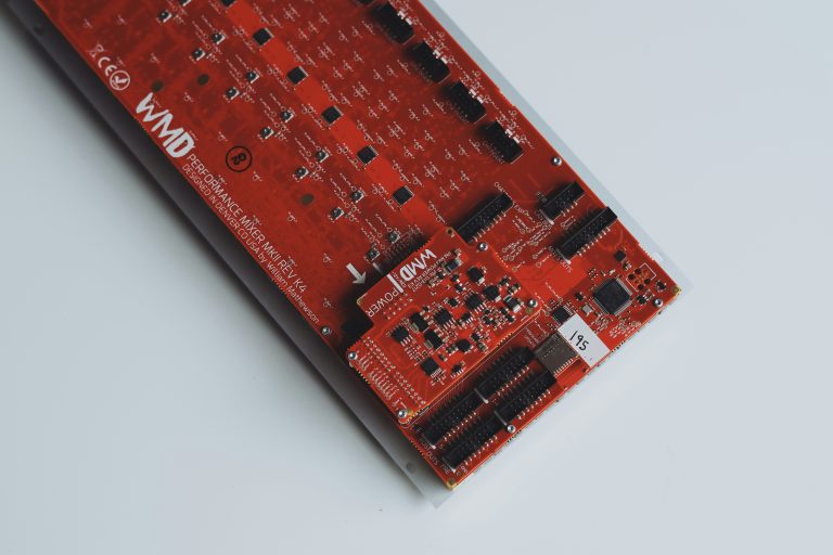
Small batch PCB production refers to manufacturing 10 to 250 pieces of a printed circuit board after prototype verification, serving as a pilot run before high-volume production. Unlike prototyping (1–10 pieces) that focuses on functional verification, small batch PCB production emphasizes process consistency, quality repeatability, and manufacturability validation. As part of our high-speed PCB prototyping service ecosystem, small batch production is the essential bridge to mass production.
The primary goals of small batch PCB production are: process validation – verify consistent manufacturability; market testing – supply early units for customer evaluation; early inventory – build initial stock for pilot customers; risk reduction – identify production issues before scaling.
Small batch PCB production is not a single fixed quantity but a range of options tailored to different project stages. For most hardware startups and engineering teams, the 50–100 piece range offers the best balance between cost and confidence.
Quantity Options & Application Scenarios
。10–20 pieces 68
Selection guidance: Start with 10–20 pieces for initial design verification; move to 20–50 pieces for customer feedback; use 50–100 pieces for full process validation; consider 100–250 pieces when demand is confirmed and design is stable.
Prototype vs Small Batch vs Mass Production
Understanding the differences helps you choose the right service. For detailed manufacturing capabilities, refer to PCB Manufacturing.
| Quantity Range | Typical Application | Key Considerations |
|---|---|---|
| Functional prototypes, internal validation, engineering tests | Lowest volume, fast turnaround (3–5 days), basic functional testing | |
| 20–50 pieces | Customer trials, small-scale market testing, beta units | Balanced cost and coverage, representative sample size |
| 50–100 pieces | Early production runs, pilot programs, regulatory samples | Full process validation, statistical confidence, DFM verification |
| 100–250 pieces | Ramp-up batches, initial mass production, channel fill | Transition to volume pricing, extended testing, vendor qualification |
| Comparison Item | Prototype | Small Batch | Mass Production |
|---|---|---|---|
| Quantity | 1–10 pieces | 10–250 pieces | 500+ pieces |
| Primary Goal | Function verification | Process validation | Cost optimization |
| Unit Price | High | Medium-High | Low |
| Process Verification | Basic | Complete | Full |
| Design Changes | Easy | Moderate | Difficult / Expensive |
| Lead Time | 3–5 days | 7–12 days | 2–4 weeks |
Real-world cost example: 10 pieces prototype ~$13 per board; 200 pieces small batch ~$209 total → $1.05 per board. Cost reduction: over 90% from prototype to small batch.
💡 Key insight: Many customers jump directly from prototype to mass production without a small batch pilot run. This often leads to unexpected yield issues, hidden process problems, and costly rework. A dedicated small batch PCB production run identifies these problems early, saving significant time and money.
Core Advantages of Small Batch Production
1. Cost Effectiveness – Amortizes fixed costs over more boards than prototype services.
2. Design Flexibility – Allows moderate modifications between batches, critical for hardware startups.
3. Faster Time-to-Market – 7–12 day lead times enable early revenue generation.
4. Quality Assurance – Uses same production lines and quality systems as mass production.
5. Customization and Special Requirements – Ideal for medical, aerospace, and industrial equipment.
6. Seamless Scalability – Same factory handles prototype, small batch, and mass production, eliminating technology transfer risk.
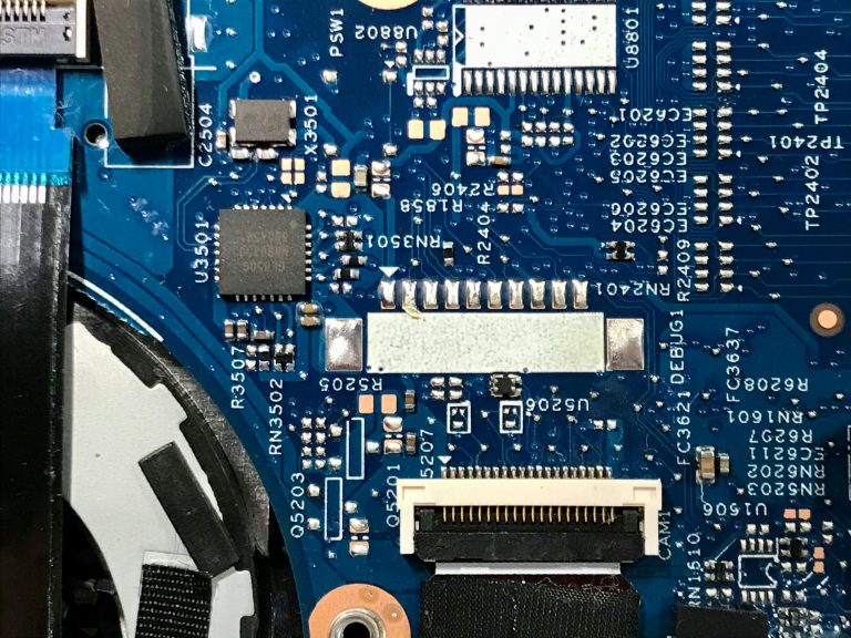
Technical Specifications & Manufacturing Capabilities
For impedance formulas, refer to Impedance Matching. For material data, see High-Speed PCB Material.
| Parameter | Capability |
|---|---|
| Layer Count | 4–32 layers |
| Board Materials | FR4, High-speed laminates, Hybrid stackups |
| Impedance Control | ±10% standard (±7% / ±5% optional) |
| Special Processes | Backdrilling, HDI, Sequential lamination, Blind/buried vias |
| Surface Finish | ENIG, HASL-LF, OSP, ENEPIG, Immersion Silver, Immersion Tin |
| Testing | AOI, Flying probe, TDR impedance test, X-ray, Four-wire Kelvin |
⚠️ Note: For high-speed designs requiring tight impedance tolerance, specify ±7% or ±5% and request TDR test reports with your small batch PCB production order.
Cost Structure & NRE Analysis
Fixed Costs (NRE): CAM & panelization, tooling & fixtures, setup & programming, DFM review – amortized across batch quantity.
Variable Costs: Material cost, processing cost, assembly cost, testing cost, logistics.
| Batch Size | Total Unit Cost (Example) | Reduction vs 10pcs |
|---|---|---|
| 10 pcs | $13.00 | Baseline |
| 50 pcs | $6.50 | 50% lower |
| 200 pcs | $5.05 | 61% lower |
| 1,000 pcs | $3.25 | 75% lower |
💡 Cost-saving tips: Combine multiple designs on one panel; use standard materials; plan batch before design freeze; request consolidated shipping.
Complete Production Workflow
Step 1: Submit Gerber files, BOM, and coordinates
Step 2: DFM & engineering review – automated analysis checks design rules
Step 3: Material procurement – laminates, prepreg, copper foil, components sourced
Step 4: PCB fabrication – imaging → etching → AOI → lamination → drilling → plating
Step 5: Electrical testing – flying probe for continuity; TDR for impedance
Step 6: Assembly (if required) – solder paste → pick-and-place → reflow → AOI
Step 7: Final inspection & packaging – visual inspection, cleanliness testing
Step 8: Documentation & shipment – certificate of compliance, test reports, material traceability
Common Challenges & Engineering Solutions
Proper Return Path design is critical for high-speed signals in small batch PCB production. Below are typical challenges and solutions:
ChallengeSolution High unit costAmortize NRE over larger batches; combine designs on one panel Component sourcing delaysUse manufacturer’s inventory parts; plan lead time Quality inconsistencyIPC Class 2/3 standards; request test reports Impedance deviationSpecify tolerance; request TDR test report Transition risk to mass productionUse same factory for prototype to mass production
How to Choose the Right Small Batch Manufacturer
1. DFM Automation & Engineering Support – Free automated DFM analysis and responsive support.
2. Component Sourcing Capability – Source from major distributors; approved vendor list.
3. Transparent Pricing – Accurate online quotation; NRE costs clearly separated.
4. Quality & Process Control – IPC, UL, ISO certifications; full traceability.
5. Testing Capabilities – Flying probe, AOI standard; TDR for high-speed designs.
6. Seamless Scalability – Same factory handles prototype, small batch, and mass production.
7. Lead Time & Communication – Reliable lead times and proactive communication.
DFM Optimization & Best Practices
Panelization Strategy: Use V-scoring or tab routing; add tooling holes and fiducial marks; leave 5–10mm edge clearance.
BOM Optimization: Prefer standard values and common packages (0402, 0603, 0805); avoid long lead time parts.
Layer Stackup: Use symmetrical stackup to prevent warpage; specify dielectric thickness based on impedance.
Design Rules: Via-to-copper clearance ≥0.2mm; trace-to-trace spacing ≥0.1mm (4mil).
Documentation: Include readme files; provide assembly drawing; specify test points for flying probe.
Complete Small Batch PCB Production Checklist
| ✅ | Item |
|---|---|
| ✅ | Gerber RS-274X format (all layers) |
| ✅ | Drill files (Excellon format) and IPC netlist |
| ✅ | BOM with manufacturer part numbers and coordinates |
| ✅ | Material type, layer count, and stackup confirmed |
| ✅ | Impedance requirements and tolerance specified |
| ✅ | Surface finish selected (ENIG recommended) |
| ✅ | Backdrilling or HDI requirements noted |
| ✅ | IPC Class (2 or 3) specified |
| ✅ | Quantity and lead time confirmed |
Key Takeaways for Small Batch PCB Production
- Small batch PCB production (10–250 pieces) bridges prototype validation and mass production
- Quantity selection depends on project stage: 10–20 for internal tests, 20–50 for customer trials, 50–100 for pilot runs
- Cost advantage comes from amortizing NRE over more boards – unit cost drops >90% from 10 to 200 pieces
- Technical capabilities match mass production: up to 32 layers, impedance control (±10% to ±5%), backdrilling, HDI
- DFM optimization directly reduces cost and improves yield
- Seamless transition – using the same factory eliminates technology transfer risk
- TDR impedance testing is recommended for high-speed designs
Frequently Asked Questions (FAQ)
Q1: What is the typical quantity range for small batch PCB production?
Small batch PCB production typically covers 10 to 250 pieces, with flexible options for gradual ramp-up.
Q2: How much does small batch production cost per board?
Cost depends on layer count, board size, and quantity. Example: 10 pieces ~$13/board; 200 pieces ~$5/board. Get a custom quote for accurate pricing.
Q3: How long does small batch production take?
Typical lead time is 7–12 days depending on layer count, material availability, and special processes.
Q4: Can I get impedance control for small batch orders?
Yes. ±10% impedance control is standard. ±7% and ±5% are available for high-speed designs. Request TDR test reports for verification.
Q5: What testing is included in small batch production?
Standard testing includes AOI and flying probe (continuity/isolation). Optional tests include TDR impedance, X-ray, and four-wire Kelvin.
Q6: Why should I use the same factory for prototype and small batch?
Keeping production in one factory eliminates technology transfer risk, ensures consistent quality, and allows process optimization to carry over to mass production.
Q7: Can small batch production include PCB assembly?
Yes. Most small batch PCB production services offer turnkey or consigned PCB assembly with pick-and-place, reflow, and AOI inspection.
Q8: What is the minimum order quantity (MOQ) for small batch?
MOQ is typically 5–10 pieces for fabrication and 10–20 pieces for assembly, depending on the manufacturer.
Get Your Small Batch PCB Production Quote
Ready to move your project from prototype to pilot production? Our small batch PCB production service supports 10 to 250 pieces with full engineering support, impedance control, and seamless transition to mass production.
What we offer: 4–32 layer PCBs with full material traceability; Impedance control: ±10% standard, ±7% / ±5% optional; Backdrilling, HDI, and hybrid stackup capabilities; Comprehensive testing: AOI, flying probe, TDR, optional X-ray; Turnkey PCB assembly with component sourcing; Same-factory continuity from prototype to mass production; ISO 9001 certified, IPC Class 2/3 compliant.
📧 Send your Gerber files, BOM (for assembly), quantity target, layer count, board dimensions, material preference, impedance requirements, and target lead time – we will provide a free DFM review, process recommendations, and a competitive quotation within 24 hours.
© 2026 HighSpeedPCBs