Welcome to the world of High Speed PCB Design. This comprehensive guide synthesizes the most trusted industry advice, equipping you with foundational knowledge to design reliable, high-performance printed circuit boards. Whether you are a student, hobbyist, or professional engineer, mastering high speed PCB design starts here.
What is High Speed PCB Design? (And Why Should You Care?)
Before diving into the “how,” it’s crucial to understand the “what” and “why.” High speed PCB design is triggered by rise time (or fall time) of a signal, not solely clock frequency. A signal with a very fast rise time, even at a relatively low clock frequency, behaves as a high-speed signal. The rule of thumb: if propagation delay of the signal trace is greater than 1/6 (or 1/4) of the signal’s rise time, you must treat it as a transmission line. This is because the signal’s edge contains high-frequency harmonics that interact with the physical geometry of the PCB.
Why It Matters: The Consequences of Ignoring High-Speed Effects
If you ignore these effects, your board may suffer from Signal Integrity (SI) issues: reflections, ringing, overshoot, undershoot causing logic errors, data corruption, system crashes. Electromagnetic Interference (EMI): poorly designed traces act as antennas, radiating energy interfering with other electronics, violating regulatory compliance (FCC, CE). Crosstalk: unwanted coupling of energy between adjacent traces causing false switching. Timing Violations: skew between clock and data signals leads to setup/hold time violations, rendering circuit non-functional. In short, a high-speed design ignoring these principles will likely fail. Mastering these concepts ensures your design works correctly, passes EMC testing, and reaches market faster.
Core Principles for Your First High Speed PCB Design
This section outlines fundamental concepts you must grasp. Think of these as your design commandments. Every high speed PCB design relies on transmission line theory, proper stackup, and routing discipline.
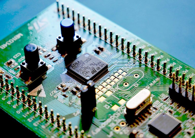
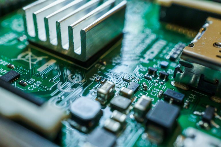
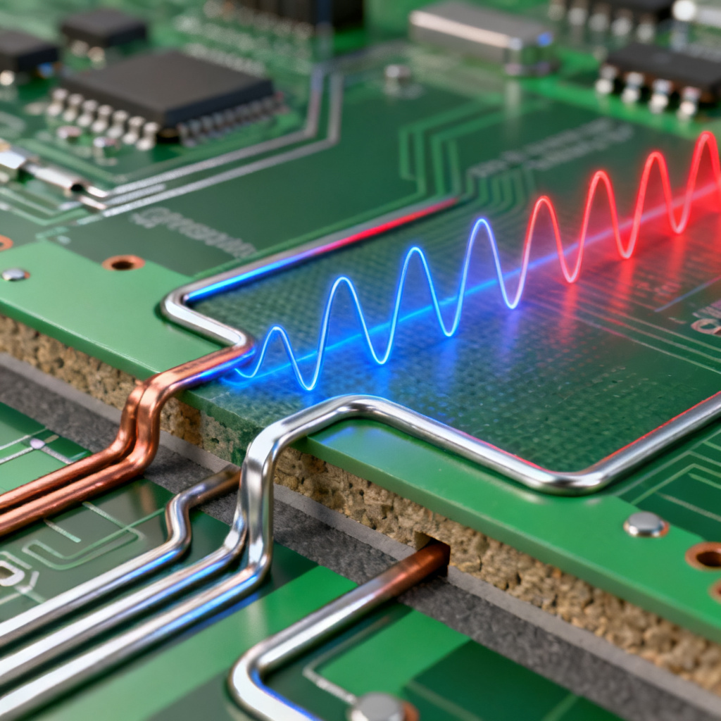
1. The Transmission Line: Your Trace is Not a Wire
At high speeds, a PCB trace becomes a transmission line with four key parameters: Resistance (R), Inductance (L), Conductance (G), Capacitance (C). The most critical parameter is Characteristic Impedance (Z0). It’s the instantaneous impedance a signal “sees” as it travels down a uniform trace. To avoid reflections, source impedance, trace impedance, and load impedance must be matched. Common target: 50Ω single-ended, 90Ω or 100Ω differential. Control impedance by using a reference plane (solid, unbroken ground or power), maintaining constant trace width, and working with your fabricator.For step-by-step impedance calculations using Polar Si9000 and Saturn PCB Toolkit, refer to our impedance matching PCB resource.
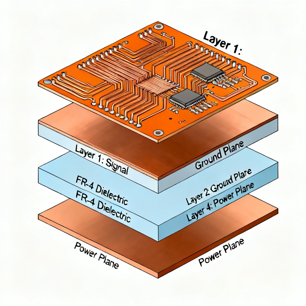
2. The Critical Role of the Stackup
Your PCB stackup is the foundation of your high speed PCB design. A proper stackup is non‑negotiable. Always have a solid reference plane. For a 4‑layer board: Top (Signal) → Ground Plane → Power Plane → Bottom (Signal). Use thin dielectric layers (e.g., 4‑5 mils) for tighter coupling, lower impedance, reduced EMI. Symmetry prevents warp. Place fastest signals on layers adjacent to a solid ground plane.
3. Routing Best Practices: The Art of the Trace
How you physically route traces is where theory meets practice. Avoid 90‑degree corners; use 45‑degree chamfered corners or arcs. Minimize via usage – every via creates impedance discontinuity. Keep traces short and direct. Maintain consistent routing density. For differential pairs, maintain constant spacing and length matching.
4. Managing Crosstalk
Crosstalk is unwanted coupling between adjacent traces. Increase trace spacing (3W rule minimum). Use guard traces connected to ground with vias. Route sensitive signals on different layers with a ground plane between. Avoid long parallel runs.
5. Power Integrity (PI): The Foundation of a Clean Signal
Noise on power supply directly translates to signal noise. Use decoupling capacitors (0.1µF, 0.01µF) placed as close as possible to IC power pins. Bulk capacitors (10µF, 100µF) handle lower‑frequency transients. Power and ground planes form a natural capacitor. Minimize loop area to reduce inductance and radiated emissions.
Your Step-by-Step High Speed PCB Design Workflow
Follow this practical workflow for your first high speed PCB design project.
Step 1: Define the Rules and Constraints
Before opening your EDA software, write down critical design rules: net classes, impedance targets (50Ω single‑ended, 100Ω differential), length matching tolerances, spacing rules, via restrictions.
Step 2: Component Placement is King
Placement is the single most important step. Read the datasheet, group by function, minimize trace lengths. Place decoupling capacitors first – smallest, most critical caps right next to IC power pins. Keep analog and digital sections separate.
Step 3: Route the Critical Nets First
Route the most sensitive, high‑speed signals first: clocks (shortest, most direct path), high‑speed data buses (DDR, PCIe, USB), then other high‑speed signals, finally low‑speed signals.
Step 4: Route the Power and Ground
Once signals are routed, pour power and ground planes using copper polygons. Connect with plenty of stitching vias. For mixed‑signal designs, use star grounding at the ADC/DAC chip.
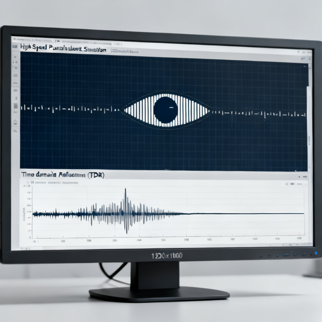
Simulation, Verification, and Common Pitfalls in High Speed PCB Design
Simulation is your best friend for high speed PCB design. Pre‑layout simulation helps determine ideal impedance and termination. Post‑layout simulation extracts parasitic R, L, C and reveals impedance mismatches, crosstalk, timing issues. Most modern EDA tools (Altium Designer, Cadence Allegro, KiCad) have built‑in simulation capabilities.
Common Beginner Mistakes (and How to Fix Them)
- Ignoring return paths: Always ensure continuous, low‑impedance return path directly underneath the signal.
- Using too many vias: Each via adds inductance. Use sparingly.
- Routing over split planes: Never route a high‑speed signal across a split in ground or power plane.
- Poor decoupling: Place caps close to IC power pins, minimize via inductance.
- Forgetting the fabricator: Provide clear stackup, impedance requirements, and tolerances in fabrication notes.
High Speed PCB Design Specifications (Structured Table)
| Parameter | Typical Value (High Speed PCB Design) | Notes |
|---|---|---|
| Impedance (single‑ended) | 50 Ω ± 10% | Controlled by trace width & dielectric |
| Impedance (differential) | 90 Ω / 100 Ω | For USB, PCIe, DDR |
| Trace spacing (3W rule) | ≥ 3× trace width | Reduces crosstalk |
| Dielectric thickness (core/prepreg) | 4–5 mils (for tight coupling) | Thinner = better SI |
| Via count per critical net | ≤ 2 (prefer 0–1) | Minimize impedance discontinuity |
Industry Terminology Explained
- Signal Integrity (SI): Quality of electrical signal in terms of timing, noise, and shape.
- Electromagnetic Interference (EMI): Unwanted radiation from PCB affecting other devices.
- Crosstalk: Unintended coupling of energy between adjacent traces.
- Characteristic Impedance (Z0): Instantaneous impedance of a uniform transmission line.
- Decoupling Capacitor: Local charge reservoir that stabilizes power supply.
- Back‑drilling: Removing unused via stub to reduce antenna effect.
Frequently Asked Questions About High Speed PCB Design
What is the most important rule in high speed PCB design?
Ensure every high‑speed signal has a continuous, low‑impedance return path directly underneath on an adjacent reference plane. Ignoring return paths is the most common mistake in high speed PCB design.
How do I choose the right stackup for high speed PCB design?
Use a symmetrical stackup with solid ground/power planes adjacent to signal layers. Thin dielectric layers (4–5 mils) improve impedance control and reduce EMI. Always consult your fabricator.
What is the difference between clock frequency and rise time in high speed PCB design?
High speed is defined by rise time, not clock frequency. A signal with fast edges contains high‑frequency harmonics that require transmission line treatment. Even a low‑frequency clock with fast rise time must be designed as high speed.