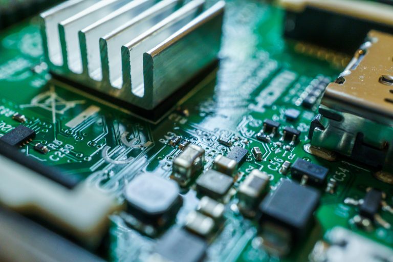
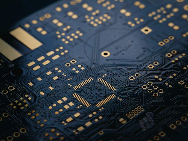
BGA fanout techniques are among the most critical and challenging steps in high-density and high-speed PCB layout. As modern ICs keep shrinking ball pitch from 1.0mm down to 0.4mm and even 0.35mm, traditional routing methods can no longer meet design and manufacturability requirements. Mastering BGA fanout techniques is essential for every PCB designer working with fine-pitch components.
This ultimate pillar guide covers all mainstream BGA fanout techniques: standard dog-bone through-hole fanout, mixed blind via routing, via-in-pad (POFV), microvia HDI, any-layer HDI, and semiconductor substrate-level fanout. You will learn pitch-based fanout selection rules, design parameters, stackup & layer count estimation, high-speed signal integrity rules, decoupling capacitor placement, DFM checklist, and common design mistakes. Applying proper BGA fanout techniques directly impacts your board’s manufacturability and signal integrity.
Table of Contents
- 1. What Is BGA Fanout & Why It Matters
- 2. BGA Ball Pitch Classification & Corresponding Fanout Strategy
- 3. Dog-Bone Fanout: Standard Through-Hole Method
- 4. Via-in-Pad (POFV) & Microvia HDI Fanout for Fine-Pitch BGA
- 5. BGA Escape Routing Principles & PCB Layer Count Estimation
- 6. High-Speed BGA Fanout Signal Integrity Design Considerations
- 7. Decoupling Capacitor Placement Rules for BGA Area
- 8. Common BGA Fanout Design Mistakes & How to Avoid Them
- 9. BGA Fanout DFM Complete Checklist
- 10. Key Takeaways & Core Design Summary
- 11. BGA Fanout FAQ
- 12. Get Professional BGA Fanout Design & DFM Review Support
What Is BGA Fanout & Why It Matters
Definition of BGA Fanout
BGA fanout techniques refer to the fundamental PCB routing strategy that routes dense BGA component pads to inner or outer PCB layers using vias and short traces. As covered in our PCB Design Guidelines, these BGA fanout techniques release routing space under the BGA package and allow signal, power, and ground pins to escape orderly to the rest of the circuit board. Selecting the right BGA fanout techniques determines your project’s success from the start.
Why BGA Fanout Is Critical
- Directly determines PCB layer count, stackup structure, and overall manufacturing cost
- Decides routing feasibility; poor fanout leads to later layout rework
- Affects high-speed signal integrity, impedance control, and power delivery performance
- Defines PCB manufacturability, production yield, and fabrication process limits
Core Challenge of Modern BGA Design
The biggest difficulty comes from continuously shrinking ball pitch: from traditional 1.0mm → 0.8mm → 0.65mm → 0.5mm → 0.4mm and below. Finer pitch means smaller pad spacing, limited trace width, and tighter via clearance, forcing designers to adopt advanced BGA fanout techniques such as HDI, microvia, and via-in-pad instead of conventional through-hole design.
BGA Ball Pitch Classification & Corresponding Fanout Strategy
BGA ball pitch is the primary factor to decide which BGA fanout techniques to use, along with fabrication process, design rule limits, and cost. Different BGA fanout techniques apply to different pitch ranges. Below is the industry standard pitch-to-fanout matching table for high-density PCB design.
| BGA Pitch | Recommended BGA Fanout Techniques | Required PCB Process | Key Design Limit |
|---|---|---|---|
| ≥ 1.0mm | Standard through-hole fanout | Conventional standard PCB | Normal trace/via rule, low cost |
| 0.8mm | Through-hole + fine trace fanout | Standard PCB with fine line | 4/4 mil line width/spacing |
| 0.65mm | Mixed blind via + through-hole | HDI 1+N+1 stackup | Blind microvia required |
| 0.5mm | Micro blind via HDI fanout | HDI 1+N+1 / 2+N+2 stackup | Resin filling optional |
| 0.4mm | Any-layer HDI fanout | Any-layer HDI process | All layers microvia |
| ≤ 0.35mm | Substrate-level fanout | Semiconductor packaging | Ultra-fine line, advanced packaging |
Core Rule: Match your BGA fanout techniques strictly to BGA pitch first; do not apply traditional through-hole fanout to 0.65mm and finer pitch BGAs. Understanding this relationship is fundamental to successful BGA fanout techniques implementation.
Dog-Bone Fanout: Standard Through-Hole Method
Dog-Bone fanout is one of the most cost-effective and widely adopted traditional BGA fanout techniques, suitable for BGA pitch ≥ 0.8mm. This BGA fanout technique features a typical pad-trace-via structure like a dog bone, easy for fabrication and mass production without HDI cost.
Recommended Design Parameters
| Design Parameter | Recommended Value |
|---|---|
| Via Hole Diameter | 0.2mm – 0.3mm |
| Via Pad Diameter | 0.45mm – 0.5mm |
| Fanout Trace Width | 4 – 5 mil |
| Maximum Fanout Trace Length | ≤ 200mil |
Layout Fanout Mode
- Outer 2~3 rows of BGA balls: fan outward to escape routing channels
- Inner BGA rows: can fan inward to inner layers or outward based on board space
- Keep trace length consistent for parallel signals to avoid timing mismatch — a key principle detailed in our High-Speed PCB Routing Rules guide.
These dog-bone BGA fanout techniques work reliably for standard-pitch components but are not suitable for fine-pitch BGAs below 0.8mm.
Via-in-Pad (POFV) & Microvia HDI Fanout for Fine-Pitch BGA
For BGA pitch ≤ 0.65mm, traditional dog-bone BGA fanout techniques cannot fit trace and via clearance. Via-in-Pad (Pad Over Filled Via / POFV) and HDI microvia fanout become the only reliable BGA fanout techniques for high-density layout. These advanced BGA fanout techniques enable fine-pitch component routing.
What Is Via-in-Pad
Via-in-pad places microvias directly on the BGA solder pad, without extending extra fanout traces. This BGA fanout technique saves massive layout space and shortens signal path length for better high-speed performance.
Manufacturing Process Requirements
- Laser drilling for ultra-small micro blind vias
- Hole wall electroplating for conductivity
- Resin via filling to flatten the pad surface
- Final surface plating (ENIG/OSP) for component soldering
HDI Stackup Matching
- 0.65mm / 0.5mm pitch: adopt 1+N+1 or 2+N+2 HDI stackup
- 0.4mm ultra-fine pitch: use Any-layer HDI for full layer interconnection
These HDI-based BGA fanout techniques enable designs that would otherwise be impossible with standard through-hole methods.
BGA Escape Routing Principles & PCB Layer Count Estimation
Escape Routing Rule of Thumb
When applying BGA fanout techniques, industry proven experience shows that every additional 2 signal layers can support fanout for 1~2 more rows of BGA pins. Early layer count planning avoids layout rework and optimizes stackup cost for effective BGA fanout techniques implementation.
BGA Pin Count vs Minimum Signal Layers
| BGA Total Pin Count | Minimum Signal Layers | Design Suggestion for BGA Fanout Techniques |
|---|---|---|
| 100 – 200 Pins | 4 – 6 Layers | Standard stackup, regular fanout适用 |
| 200 – 400 Pins | 6 – 8 Layers | Partial inner layer escape |
| 400 – 700 Pins | 8 – 10 Layers | HDI recommended |
| 700 – 1000+ Pins | 10+ Layers + HDI | Any-layer HDI or substrate |
Escape Routing Best Practice
- Route high-speed differential and clock signals first
- Assign inner layers for dense inner BGA pins
- Separate signal, power, and ground layers clearly to avoid crosstalk
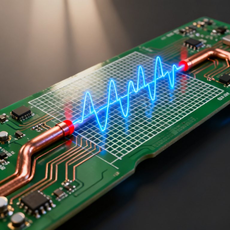
High-Speed BGA Fanout Signal Integrity Design Considerations
High-speed interfaces like DDR, PCIe, Ethernet, and SerDes require strict fanout rules beyond basic routing. For impedance control fundamentals and return path integrity within your BGA fanout techniques, see our Impedance Matching Ultimate Guide and Return Path Design Guide. Proper BGA fanout techniques must account for these SI requirements.
| Design Aspect | Key High-Speed Fanout Rules for BGA Fanout Techniques |
|---|---|
| Impedance Control | Optimize via anti-pad size; keep differential pairs tightly coupled |
| Return Path Design | Place one adjacent GND via for each high-speed signal via |
| Clock & Differential Pairs | Prioritize fanout routing; maintain symmetric trace length |
| Power & Ground Distribution | Isolate power and ground fanout zones; separate analog/digital grounds |
| Crosstalk Suppression | Keep sufficient spacing between high-speed fanout traces |
Following these SI rules within your BGA fanout techniques eliminates signal reflection, crosstalk, and timing errors in high-density BGA designs.
Decoupling Capacitor Placement Rules for BGA Area
Power integrity heavily depends on proper decoupling capacitor layout under BGA components. The short-loop design principle — minimizing parasitic inductance and suppressing high-frequency noise — is a key topic in our Power Integrity Guide and should be integrated with your BGA fanout techniques.
- Use 0402 / 0603 high-frequency decoupling capacitors
- Place capacitors on the PCB backside directly beneath the BGA
- Match each critical power pin with one corresponding decoupling capacitor
- Minimize trace length from capacitor to BGA power pin to reduce parasitic inductance
- Avoid long shared power traces; keep loop path as short and direct as possible
Short loop design in your BGA fanout techniques suppresses power noise, stabilizes voltage, and improves BGA chip operating stability.
Common BGA Fanout Design Mistakes & How to Avoid Them
| Mistake in BGA Fanout Techniques | Consequence | Solution |
|---|---|---|
| Wrong fanout method for BGA pitch | Routing impossible, rework | Match method to pitch using Section 2 table |
| Insufficient via pad clearance | DFM violation, short circuit | Follow manufacturer minimum clearance |
| Asymmetric differential pair fanout | Impedance mismatch, signal skew | Keep trace length and spacing symmetric |
| Missing GND return vias | Poor return path, crosstalk, attenuation | Add adjacent GND vias per Section 6 |
| Unreasonable decoupling capacitor placement | Power instability, noise | Place caps under BGA with shortest loop |
| Overlooking layer count planning | Insufficient routing resources, rework | Estimate layers using Section 5 table |
BGA Fanout DFM Complete Checklist
Use this checklist to validate your BGA fanout techniques before finalizing PCB design and sending files to fabrication:
- Fanout technique matches exactly with BGA ball pitch
- Via hole, via pad, and trace spacing meet PCB manufacturer DFM rules
- All differential pairs adopt symmetric fanout and matched trace length
- High-speed signal vias are equipped with nearby GND return vias
- Power and ground copper area satisfy current carrying capacity requirements
- Decoupling capacitors are placed with minimal loop length
- Complete BGA fanout layout and stackup documents prepared for factory review
- HDI microvia / resin filling process requirement checked if using via-in-pad
Key Takeaways for BGA Fanout Techniques
- BGA ball pitch is the decisive factor to select which BGA fanout techniques to use
- Dog-bone through-hole is cost-effective only for 0.8mm pitch and above
- Fine-pitch BGA (≤0.65mm) requires advanced BGA fanout techniques: via-in-pad, microvia and HDI stackup
- Layer count follows the rule: 2 extra signal layers support 1~2 more rows of BGA fanout
- High-speed fanout must focus on impedance control, return path, and differential symmetry
- BGA decoupling capacitors should be placed underneath the package with the shortest loop
- Always run DFM checklist to ensure design manufacturability — correct BGA fanout techniques save time and cost
BGA Fanout FAQ
Q1: What is the easiest BGA fanout technique for beginners?
Dog-bone through-hole fanout for 0.8mm and 1.0mm pitch BGAs is the easiest BGA fanout technique. It uses standard PCB process with simple rules and low cost, making it ideal for learning BGA fanout techniques.
Q2: Do I need HDI for 0.5mm pitch BGA?
Yes. 0.5mm pitch cannot use traditional dog-bone; HDI microvia or via-in-pad is required for feasible fanout. This is a core BGA fanout technique decision point for fine-pitch components.
Q3: What is the difference between via-in-pad and normal dog-bone fanout?
Via-in-pad puts microvia directly on the pad without extra fanout traces, saving space for fine-pitch BGA fanout techniques; dog-bone uses extended traces and standard through-hole vias.
Q4: How many PCB layers do I need for a 500-pin BGA?
Normally 8~10 layers with HDI stackup is recommended for stable fanout and signal routing when applying proper BGA fanout techniques.
Q5: Why place decoupling capacitors under the BGA?
It minimizes power supply loop length, reduces parasitic inductance, suppresses high-frequency noise, and improves power integrity — an essential consideration in BGA fanout techniques.
Get Professional BGA Fanout Design & DFM Review Support
Designing high-density BGA fanout requires rich experience in PCB stackup, DFM rules, high-speed signal integrity, and HDI manufacturing capability. A wrong fanout plan will lead to higher cost, longer lead time, or even production failure. Our team specializes in BGA fanout techniques for complex high-density designs.
We offer: Custom BGA fanout techniques scheme design • PCB stackup layer count optimization • Via size and pad clearance DFM rule checking • High-speed signal fanout consultation • HDI PCB manufacturing quotation
All design files strictly confidential. Response within one business day.
About
We are a specialized PCB design and manufacturing service provider serving industrial, automotive, medical, and communications OEMs worldwide. Our expertise in BGA fanout techniques ensures your high-density PCBs are manufacturable and electrically reliable. Trust our team to apply the right BGA fanout techniques for your next project.
© 2026 HighSpeedPCBs.com — Professional High-Speed PCB Solutions