Understanding the real difference between High Speed vs High Frequency PCB Design is critical for engineers and B2B buyers sourcing custom PCBs for export. This pillar guide clarifies material, signal integrity, and layout distinctions to help you make informed decisions.
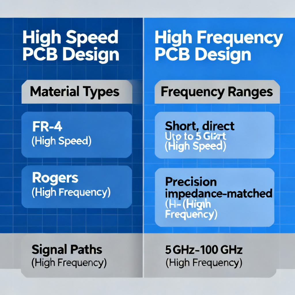
High Speed vs High Frequency PCB Design: Core Definitions
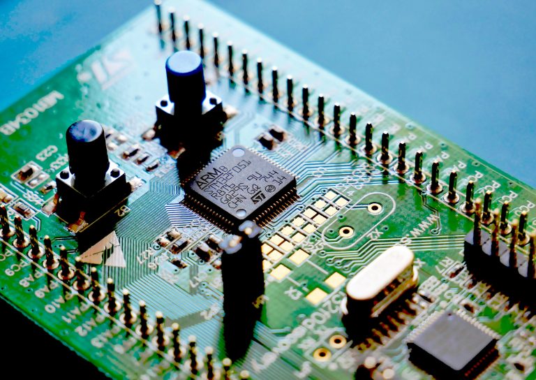
High Speed PCB Design: Defined by Rise Time
In High Speed PCB Design, the signal’s rise time relative to trace length determines the design approach. When propagation delay exceeds 20% of rise time, transmission line effects dominate. This domain focuses on timing and transient behavior.
High Frequency PCB Design: Defined by Wavelength
In High Frequency PCB Design, operating frequency above 100 MHz or 1 GHz makes wavelength comparable to PCB dimensions. The key challenges are impedance control and dielectric loss, focusing on wave propagation and electromagnetic field behavior.
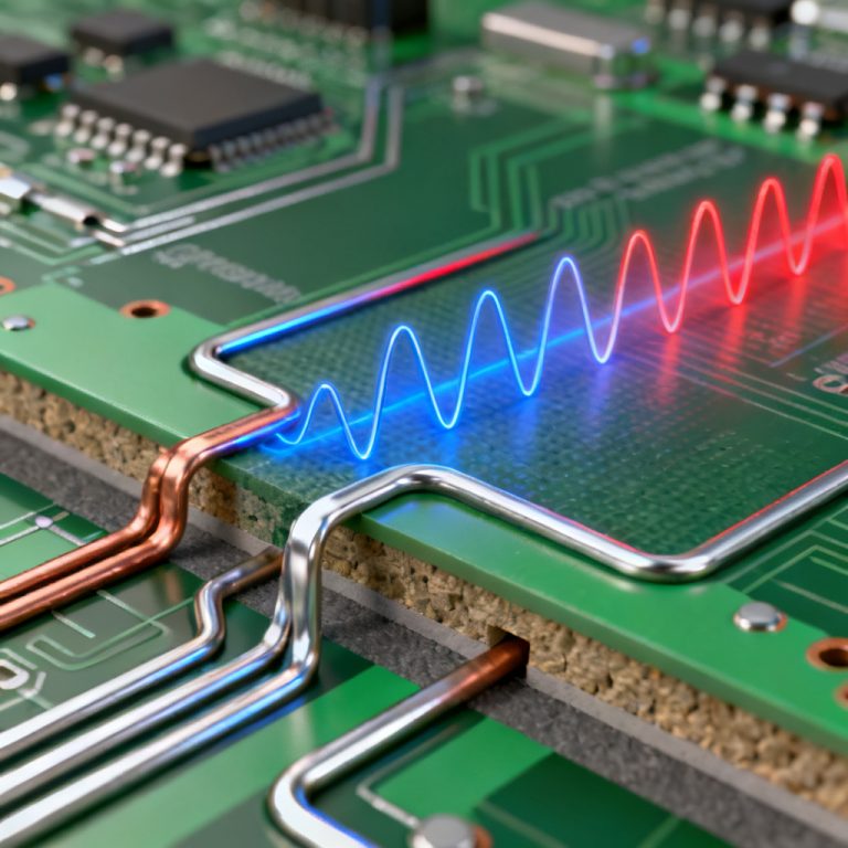
Time Domain vs Frequency Domain Control
High Speed design controls time domain parameters like skew, jitter, and setup/hold times. High Frequency design controls frequency domain parameters such as insertion loss, return loss, and phase noise. A high-speed digital signal may have low fundamental frequency but fast edges, while a high-frequency analog signal has high fundamental frequency with slow edges.
Material Selection in High Speed vs High Frequency PCB Design
Standard FR-4 vs Mid-Loss Laminates for High Speed
High Speed PCB Design often uses standard FR-4 for moderate data rates. Above 1 Gbps, mid-loss materials like Nelco 4000-13 or Isola 370HR with Df around 0.008-0.012 become necessary to control signal loss.
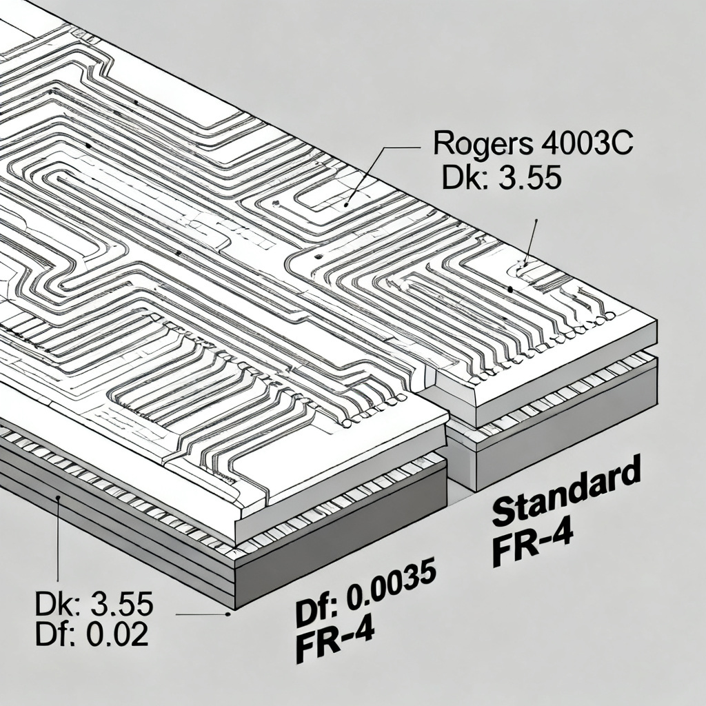
Low-Loss Laminates for High Frequency
High Frequency PCB Design demands low and stable Dk across frequency and temperature. Materials like Rogers 4003C (Dk 3.55, Df 0.0027) or PTFE-based laminates are preferred. The dissipation factor (Df) must be minimized to reduce attenuation.
Hybrid Stackups for Mixed-Signal Boards
For boards combining high-speed digital and high-frequency analog, hybrid stackups use low-loss RF laminates on outer layers and FR-4 or mid-loss materials on inner layers. This balances performance with cost but requires careful material compatibility to avoid warpage.
Signal Integrity Challenges: High Speed vs High Frequency
Reflections, Crosstalk, and Termination in High Speed
High Speed PCB Design is dominated by reflections from impedance mismatches. Solutions include proper termination (series, parallel, Thevenin), controlled impedance traces (50Ω, 100Ω differential), and back-drilling for via stubs above 10 Gbps.
Skin Effect, Dielectric Loss, and Surface Roughness in High Frequency
High Frequency PCB Design is dominated by skin effect and dielectric loss. Smooth copper foils (RTF, VLP, HVLP) and low-loss materials are essential. Insertion loss is the primary metric, and via stubs must be eliminated via back-drilling or microvias.
Grounding and Shielding: Different Approaches
Both domains require solid ground planes. In High Speed, the ground plane provides a low-inductance return path. In High Frequency, it creates a microstrip transmission line with predictable impedance and acts as a shield. Stitching via spacing must be less than λ/20 in high-frequency designs.
Layout and Routing Rules: Practical Differences
Trace Length Matching and Skew in High Speed
In High Speed PCB Design, trace length matching is critical to minimize skew. Tolerances are often ±10 mils or tighter. Differential pairs must be length-matched within the pair and between pairs, using serpentine routing for delay tuning.
Impedance Control and Stub Management in High Frequency
In High Frequency PCB Design, impedance control must account for etch factor and prepreg resin content. Stub-free via design using microvias or back-drilling is mandatory. Grounded coplanar waveguide structures reduce loss and improve isolation.
Component Placement and Isolation
For High Speed, place noisy components away from sensitive lines and use decoupling capacitors. For High Frequency, use grounded via fences or copper pour with via stitching for isolation. Keep RF traces as short as possible.
Simulation and Testing Methods
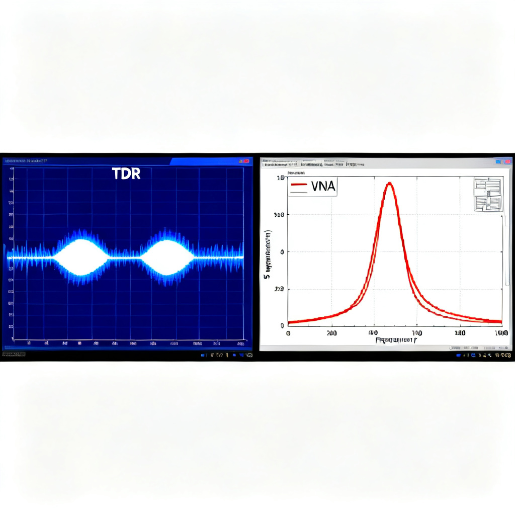
Time-Domain Reflectometry (TDR) for High Speed
High Speed designs are validated using TDR to measure impedance discontinuities and eye diagram analysis for signal quality. SPICE or IBIS simulations are standard.
Vector Network Analyzer (VNA) for High Frequency
High Frequency designs are validated using a VNA to measure S-parameters. Insertion loss and return loss are key metrics. 3D EM simulation is required for accurate modeling of vias and transitions.
Design for Manufacturing (DFM) in Both Domains
Both domains require strict DFM rules. Controlled impedance must be verified via coupon testing. Material tolerances must be specified. For high frequency, specify copper roughness and via back-drilling depth.
Cost and Manufacturing Considerations
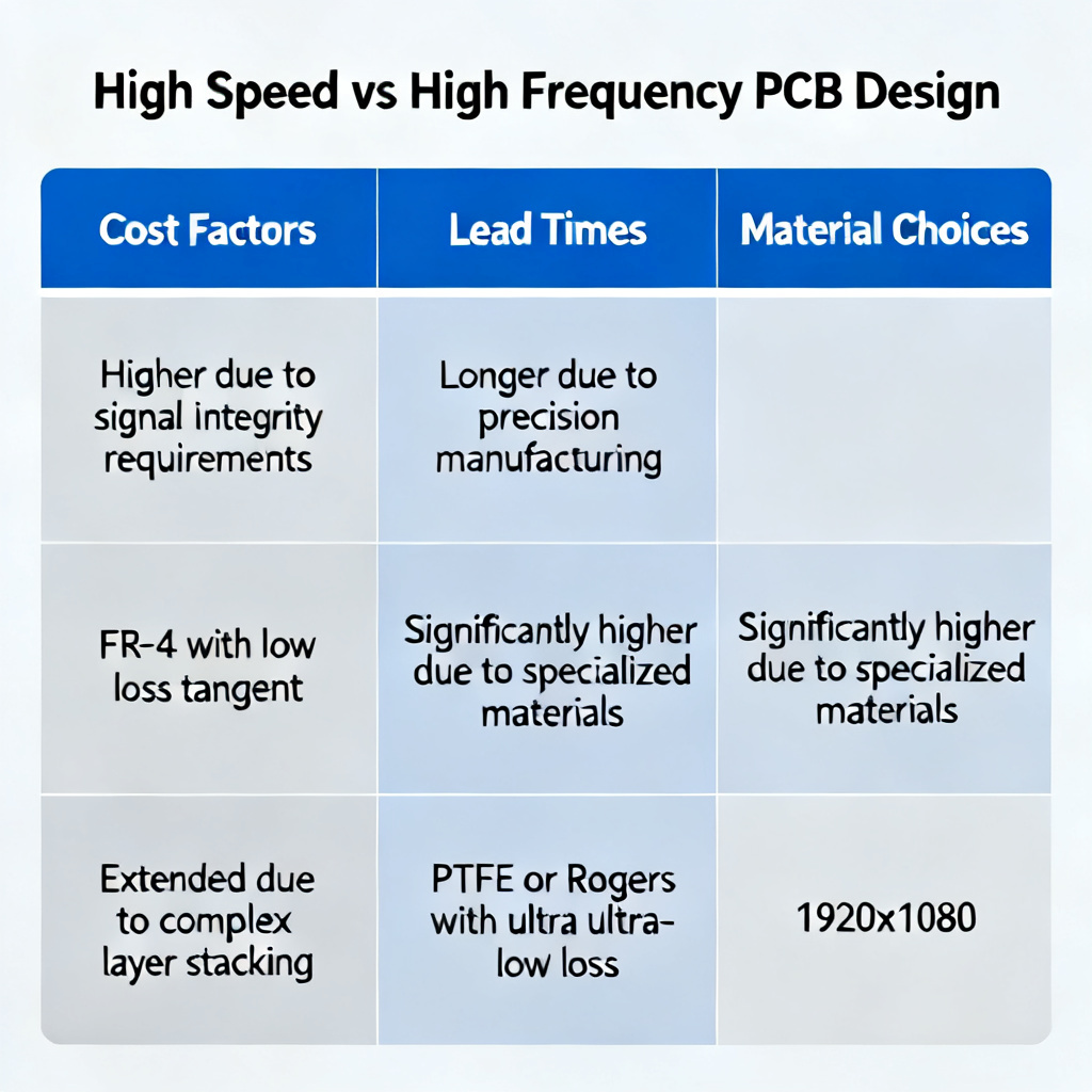
| Parameter | High Speed PCB Design | High Frequency PCB Design |
|---|---|---|
| Material Cost | Moderate (FR-4, mid-loss) | High (Rogers, PTFE) |
| Fabrication Complexity | Standard with back-drilling | Specialized lamination, smooth copper |
| Cost Increase vs Standard PCB | 10-30% | 50-200%+ |
| Lead Time | Standard | Longer due to material sourcing |
| Supplier Qualification | Standard IPC Class 2/3 | Rogers certified, IPC Class 3 |
High Speed PCB Design is cost-effective but requires careful design. High Frequency PCB Design demands premium materials and processes. Ensure your manufacturer has experience with high frequency laminates and controlled impedance testing.
Frequently Asked Questions About High Speed vs High Frequency PCB Design
What is the main difference between High Speed and High Frequency PCB Design?
The main difference is that High Speed PCB Design focuses on signal rise time and timing integrity, while High Frequency PCB Design focuses on operating wavelength and loss control. High speed is about edge rates; high frequency is about wave propagation.
Can FR-4 be used for High Frequency PCB Design?
FR-4 is generally unsuitable for High Frequency PCB Design above 1 GHz due to its high dissipation factor (Df ~0.02) and unstable dielectric constant. Low-loss laminates like Rogers or PTFE are required.
What materials are best for High Speed PCB Design?
For High Speed PCB Design, standard FR-4 works for moderate data rates. For rates above 1 Gbps, mid-loss materials like Nelco 4000-13 or Isola 370HR are recommended to control signal loss.
How does back-drilling differ in High Speed vs High Frequency designs?
In High Speed PCB Design, back-drilling removes via stubs to reduce reflections. In High Frequency PCB Design, back-drilling eliminates via stubs that cause resonances and insertion loss. Both require precise depth control.
“`