If you are a design engineer, procurement specialist, or electronics enthusiast entering the world of high-speed PCB design, the datasheet is your most critical document. This guide on how to read a high speed PCB design datasheet will teach you to extract the exact information needed to specify, design, and procure a board that works the first time.
1. The Core Structure of a High Speed PCB Design Datasheet
Every professional high-speed PCB datasheet follows a logical structure. Understanding this structure is the first step to reading it correctly. The three most trusted sources agree on the following essential sections.
1.1 Header Information
- Part Number / Model: Unique identifier for the specific PCB or laminate material.
- Revision Level: Always check the revision. A “Rev A” vs “Rev C” can mean different dielectric constants or thickness tolerances.
- Date of Issue: Ensures you are using the most current data.
- Manufacturer Details: Name, contact, and often a logo.
1.2 Material and Stack-Up Section
This is the most critical part for high-speed PCB design. Look for:
- Laminate Type: e.g., FR-4 (standard), Rogers 4350B (high-frequency), Isola 370HR, or PTFE-based materials.
- Dielectric Constant (Dk or εr): For high-speed, a stable Dk over frequency is crucial. Typical values: FR-4 = 4.2–4.5; Rogers = 3.48–3.66.
- Dissipation Factor (Df or tan δ): Measures signal loss. Target: Df < 0.01 for digital signals above 1 GHz.
- Glass Weave Style: e.g., 106, 1080, 2116, 7628. For high-speed, prefer fine weaves (106, 1080) or spread-glass styles.
- Copper Foil Type: Standard electrodeposited (ED) vs. rolled annealed (RA). RA foil has lower surface roughness, reducing skin effect losses.
1.3 Electrical Performance Specifications
- Impedance Target (Z0): Usually 50Ω single-ended or 100Ω differential. Tolerance is typically ±10% (±5% for critical designs).
- Propagation Delay: Measured in ps/inch. For FR-4, it’s roughly 180 ps/inch.
- Maximum Operating Frequency: The frequency at which the board can reliably transmit signals.
- Insertion Loss (IL): Expressed in dB per unit length. Lower absolute value is better.
- Return Loss (RL): Better than -15 dB is good; -20 dB is excellent.
- Crosstalk: Keep below -40 dB for dense high-speed designs.
1.4 Physical and Mechanical Dimensions
- Board Thickness: Total thickness. For high-speed, consistent thickness is vital for impedance control.
- Copper Weight: Typically 0.5 oz to 2 oz per square foot.
- Aspect Ratio: Ratio of board thickness to smallest hole diameter. High aspect ratios (>10:1) may require specialized plating.
- Surface Finish: For high-speed, ENIG or Immersion Silver are preferred for flatness and solderability.
2. How to Interpret the Key Parameters in a High Speed PCB Design Datasheet
Now that you know the structure, let’s dive into how to read and apply each critical parameter when learning how to read a high speed PCB design datasheet.
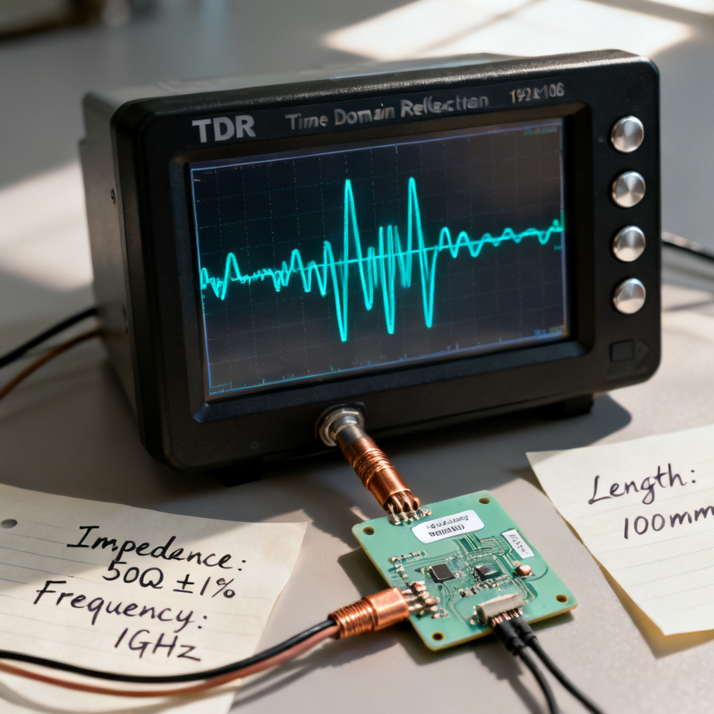
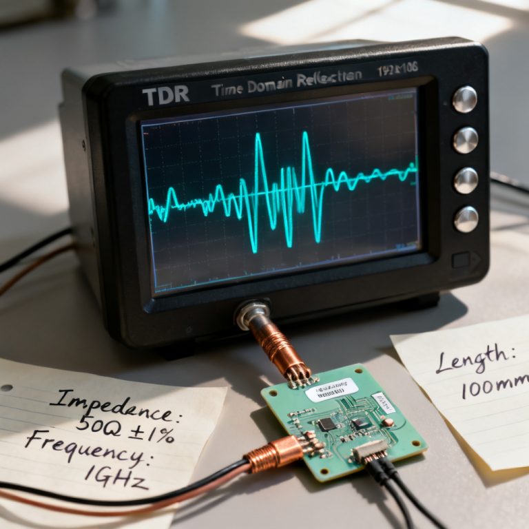
Step 1: Identify the Target Impedance and Tolerance
What to look for: A clear statement like “Target Z0 = 50Ω ± 10%”.
How to read it: Tolerance matters. ±10% is acceptable for most digital protocols. For PCIe Gen 4/5 or DDR5, you need ±5% or better. Check if impedance was measured using TDR or calculated from stack-up.
Step 2: Verify the Dielectric Material and Its Properties
What to look for: Material name, Dk and Df values at multiple frequencies.
How to read it: Stable Dk over frequency is the hallmark of a high-speed material. Df below 0.01 is good for digital signals. High Tg (>170°C) means better thermal stability.
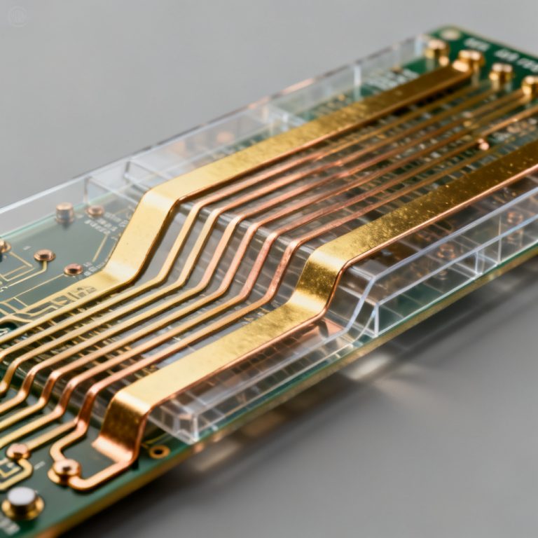
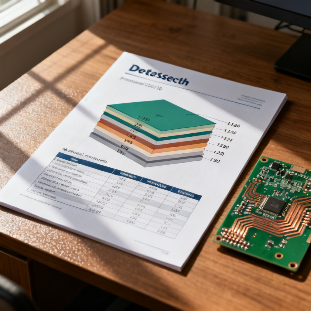
Step 3: Examine the Stack-Up and Layer Count
What to look for: A cross-section diagram showing layer order, material thickness, and prepreg/core designations.
How to read it: Every high-speed signal layer must have an adjacent solid ground or power plane. A balanced stack-up prevents warpage and ensures consistent impedance.
| Layer | Material | Thickness (mil) | Copper Weight |
|---|---|---|---|
| Top (Signal) | Prepreg (1080) | 4.0 | 0.5 oz |
| Layer 2 (GND) | Core (FR-4) | 4.0 | 1 oz |
| Layer 3 (PWR) | Core (FR-4) | 4.0 | 1 oz |
| Bottom (Signal) | Prepreg (1080) | 4.0 | 0.5 oz |
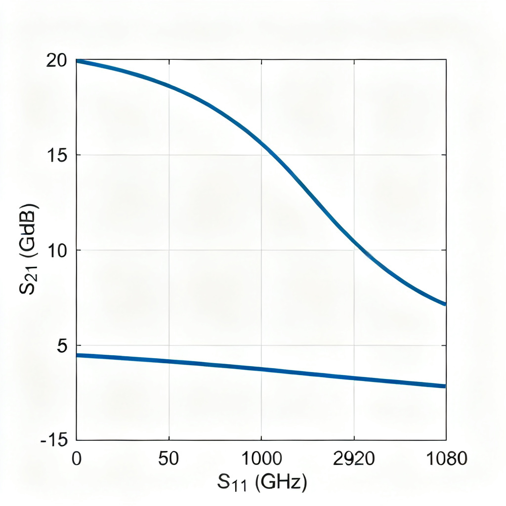
Step 4: Analyze the Insertion Loss and Return Loss Graphs
What to look for: Graphs showing Insertion Loss (S21) and Return Loss (S11) vs. Frequency.
How to read it: The Insertion Loss curve should be smooth and monotonic. Return Loss should be below -15 dB across the entire frequency band of interest.
Step 5: Check the Surface Finish and Solderability
What to look for: Finish type: ENIG, HASL, OSP, Immersion Silver, ENEPIG.
How to read it: ENIG is the gold standard for high-speed due to its flat surface. HASL is cheaper but creates uneven surfaces. Avoid OSP for high-speed designs unless assembly is immediate.
3. Common Pitfalls When Reading a High Speed PCB Design Datasheet
Even experienced engineers can miss critical details. Here are the most common mistakes when learning how to read a high speed PCB design datasheet.
Pitfall 1: Ignoring the Frequency Dependence of Dk
Problem: Using the 1 MHz Dk value for a 10 GHz design.
Solution: Always use the Dk value at your operating frequency.
Pitfall 2: Assuming All “50Ω” Traces Are Equal
Problem: Two boards both claim “50Ω impedance,” but one uses ±5% tolerance and the other uses ±15%.
Solution: Always verify the tolerance. For high-speed, demand ±5% or better.
Pitfall 3: Overlooking the Copper Surface Roughness
Problem: Standard ED copper has roughness of 1–2 μm RMS, increasing Insertion Loss above 10 GHz.
Solution: Specify low-profile copper for frequencies above 10 GHz.
Pitfall 4: Misinterpreting the “Maximum Operating Frequency”
Problem: The datasheet says “Max Frequency: 10 GHz,” but that only applies to a single trace.
Solution: Understand that “max frequency” is usually a material property, not a board-level guarantee.
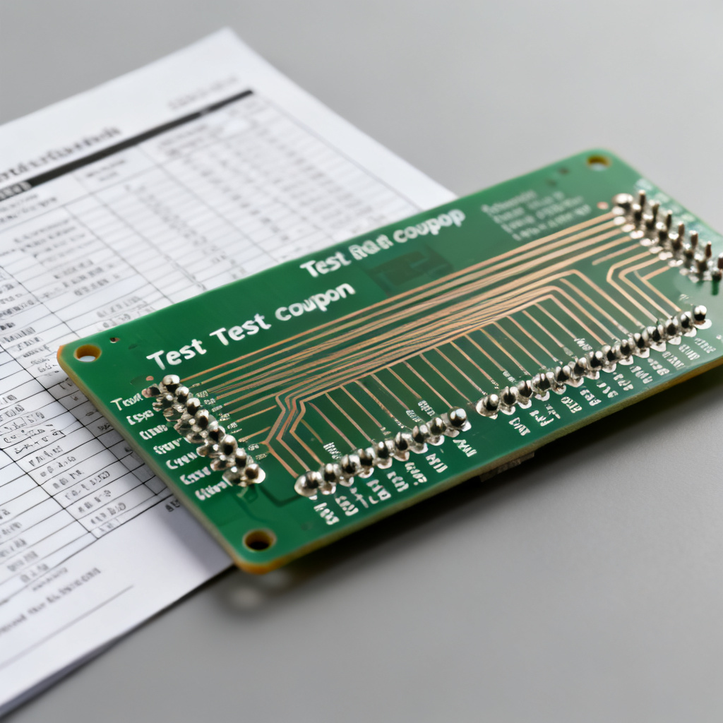
Pitfall 5: Not Verifying the Test Coupon Design
Problem: Impedance test results come from a coupon that is not representative of the actual board.
Solution: Ask for a copy of the test coupon layout.
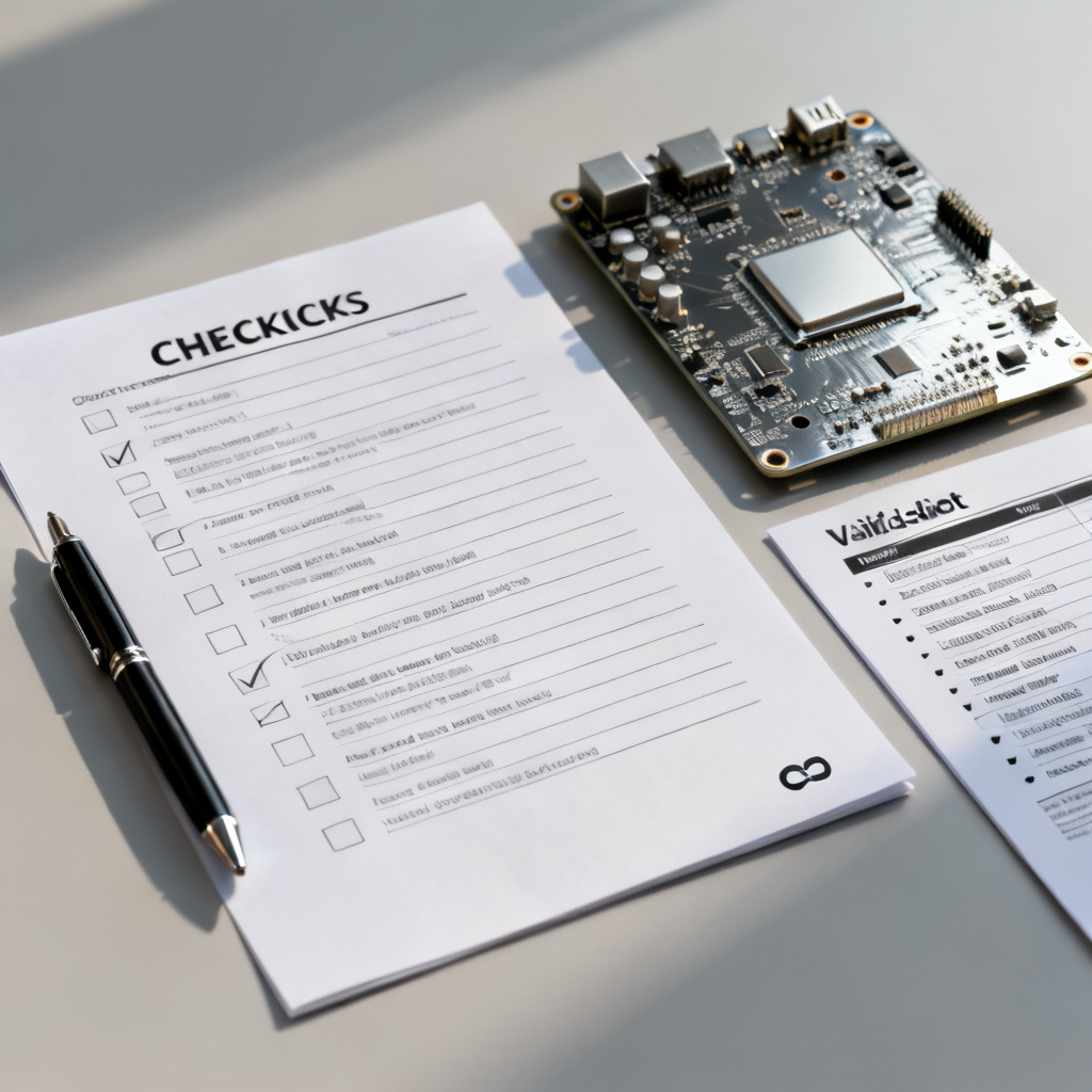
4. How to Use the High Speed PCB Design Datasheet to Validate Your Design
Once you have read the datasheet, use it to verify that your design will meet its performance goals.
Step 1: Cross-Reference the Stack-Up with Your Impedance Calculator
Use a field solver to calculate expected impedance based on the datasheet’s material properties. If your calculated impedance differs by more than 2Ω, contact the manufacturer.
Step 2: Check the Insertion Loss Budget
Calculate total Insertion Loss for your longest trace. Ensure it is within your system’s budget.
Step 3: Verify the Surface Finish Compatibility
If your assembly process uses lead-free solder, ensure the finish is compatible. ENIG and Immersion Silver work well.
Step 4: Ask for the DFM Report
A reputable manufacturer will provide a DFM report alongside the datasheet. Do not ignore this report.
5. Frequently Asked Questions About High Speed PCB Design Datasheets
Do I need a high speed PCB design datasheet for every PCB?
No. Only for boards carrying digital signals above 100 MHz or with rise times faster than 1 ns.
What is the difference between a datasheet and a fabrication drawing?
The datasheet provides material and performance specifications. The fabrication drawing is a mechanical blueprint. Both are needed for high-speed PCB production.
Can I trust a datasheet that doesn’t include test data?
No. A professional high-speed PCB design datasheet always includes measured test data.
How do I know if a material is high-speed vs. standard?
Look for Df < 0.01, stable Dk across frequency, and a Tg > 170°C.
What if the datasheet says “Impedance: 50Ω ± 10% (typical)”?
“Typical” is not a guarantee. Always request guaranteed or measured values.
6. Conclusion: Your Action Plan for Reading a High Speed PCB Design Datasheet
Reading a high speed PCB design datasheet is a core skill for high-speed PCB design, combining material science, electrical engineering, and manufacturing knowledge. By following this guide, you can identify the correct material, verify that impedance and loss meet your targets, avoid common pitfalls, and validate your design before fabrication.
Next Steps: Download a sample high-speed PCB datasheet from a reputable manufacturer. Practice reading it using the checklist above. Contact our team if you need a custom high-speed PCB datasheet tailored to your specific project.
“`