Abstract
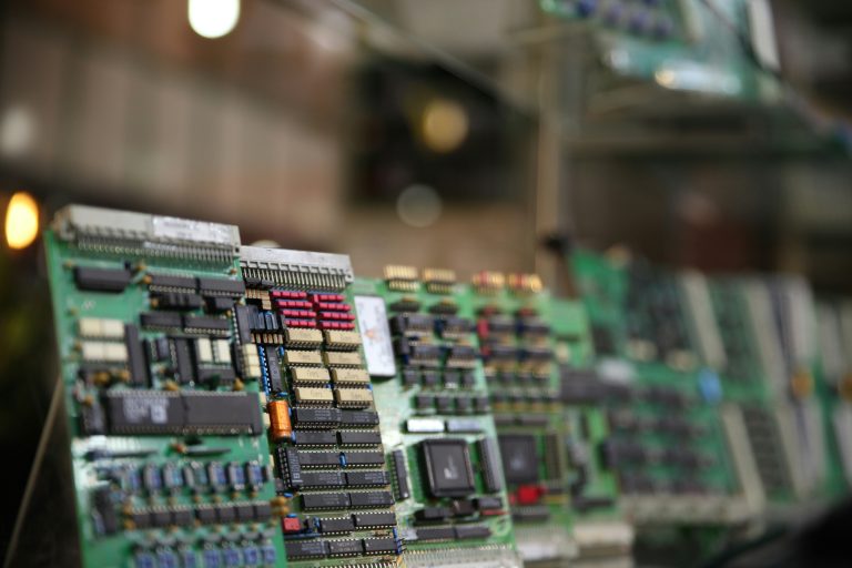
With the rapid advancement of high-speed serial communication, high-capacity data storage, high-definition video transmission, and high-performance computing hardware, high-speed PCB design has become the core foundation of modern electronic products. As signal speeds continue to increase, traditional conventional routing methods easily cause signal reflection, crosstalk, timing distortion, and electromagnetic interference, leading to unstable operation, data loss, and low mass production yield.
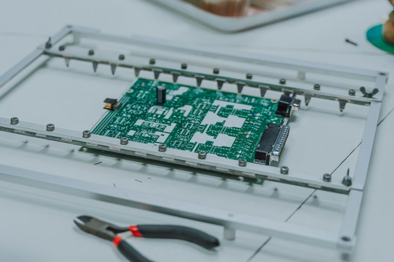
This complete pillar article delivers a systematic, practical, and industry-standard guide for hardware engineers, layout designers, R&D teams, and industrial buyers. It covers full lifecycle high-speed PCB design knowledge, including PCB stackup design, impedance matching, differential pair routing, BGA fanout design, high-speed via optimization, PCB grounding design, high-speed interface layout, and PCB DFM guidelines.
All content adopts neutral industry perspectives, integrates universal design principles and mass-production experience, and balances professional depth with easy reading. We also provide professional PCB design audit, customized stackup solution, process optimization and accurate quotation services for global business clients.
1. Introduction to High-Speed PCB Design
1.1 How to Define a High-Speed PCB
Most designers judge high-speed circuits simply by operating frequency. However, the professional industry standard is based on signal rise time and transmission delay.
A printed circuit board is defined as high-speed when the signal rise time is less than 6 times the trace propagation delay. At this stage, obvious transmission line effects will appear and directly affect signal integrity.
Practical Industry Classification Standard
- 50MHz and above: Basic high-speed protection and complete reference plane management are required.
- 100MHz / 1Gbps and above: Full high-speed design constraints and standardized routing must be fully implemented.
- 25Gbps and above: Low-loss dielectric materials, stub removal technology, HDI and length matching are essential.
Even if the overall working frequency is low, fast edge switching will still produce high-frequency harmonic noise. High-speed design is a systematic project of overall noise suppression, shielding processing and electromagnetic compatibility optimization.
1.2 Standard High-Speed PCB Design Process
A standardized closed-loop design process effectively reduces repeated revisions and lowers mass production risks.
Pre-Design Planning
Evaluate PCB layer quantity according to product specifications, signal density and power demand; select high-frequency low-loss materials; complete symmetric stackup planning; confirm fixed impedance values for different signal types; classify key high-speed networks in advance and reserve independent routing and shielding areas.
Layout & Constraint Routing
Complete reasonable component zoning; centrally arrange high-density chips and high-speed connectors; strictly follow impedance standards, spacing limits and length matching requirements during routing; reduce layer switching and unnecessary vias; keep sensitive high-speed signals away from high-power and high-frequency interference sources. This step-by-step workflow is the backbone of successful high-speed PCB design.
1.3 Common and Dangerous Design Mistakes
- Only focusing on circuit connectivity while ignoring signal return paths, resulting in large radiation loops.
- Adding vias randomly and switching layers frequently, causing impedance discontinuity and signal loss.
- Unbalanced differential length and unstable spacing, resulting in severe common-mode noise and EMI problems.
- Splitting ground or power planes arbitrarily, cutting off complete return paths for high-speed signals.
- Routing based solely on experience without impedance calculation and material parameter verification.
- Ignoring factory process limits, resulting in poor production yield and increased overall cost.
2. PCB Stackup Design for High-Speed Signals
PCB stackup design is the foundation of high-speed design. A scientific and reasonable layer structure can solve more than 60% of signal interference and EMC risks. Unreasonable stacking will cause long-term data errors, network instability and radiation over-standard problems.
2.1 How to Choose the Right PCB Layer Count
The number of layers is determined comprehensively by signal density, transmission speed, power quantity, shielding demand and cost budget.
- 4 Layers: Cost-effective high-speed solution, suitable for devices within 1Gbps.
- 6–8 Layers: The most popular mainstream structure, widely used in industrial equipment, communication hardware and vehicle electronics.
- 10–12 Layers: High-density advanced solution for high-speed storage, multi-channel differential signals and high-performance computing.
- 14+ Layers: Custom high-end stacking with ultra-low-loss materials for server and high-frequency precision equipment.
2.2 Classic Universal Stackup Structure
The core principle: All high-speed signal layers must be adjacent to complete ground planes to form stable shielding.
| Layer Count | Standard Stackup Structure | Application Features |
|---|---|---|
| 4-Layer | Signal – GND – Power – Signal | Basic high-speed structure, stable impedance and power performance |
| 6-Layer | Signal – GND – Signal – Signal – GND – Signal | Dual ground shielding, strong crosstalk suppression for multi-differential designs |
| 8-Layer | Signal – GND – Signal – GND – Power – Signal – GND – Signal | High-performance universal stack, multi-layer isolation for complex high-speed products |
2.3 Mandatory Symmetric Stackup Principle
All medium and high-end high-speed PCBs must adopt central symmetric stackup.
With the middle layer as the central axis, the copper thickness, dielectric thickness and material structure remain completely consistent on both sides.
Core Advantages
- Effectively prevent board warpage and deformation during high-temperature soldering and lamination.
- Balance interlayer dielectric parameters to ensure stable impedance of all traces.
- Avoid timing deviation and data error caused by asymmetric materials.
2.4 Core and Prepreg Material Features
- Core: Fully cured rigid substrate with stable dielectric parameters, used for inner power and ground planes.
- Prepreg: Semi-cured adhesive material with adjustable thickness, used for lamination and fine adjustment of dielectric thickness.
For ultra-high-speed scenarios, low-Dk and low-Df high-performance materials are recommended to reduce high-frequency signal attenuation. A well-planned stackup is the foundation of reliable high-speed PCB design.
3. PCB Impedance Control and General Routing Rules
Accurate and stable PCB impedance control is the core of reliable high-speed signal routing. Sudden impedance changes will directly cause signal reflection, waveform distortion, data bit errors and link disconnection.
3.1 Universal Industry Standard Impedance
| Signal Type | Target Impedance | Typical Application |
|---|---|---|
| Single-Ended Signal | 50Ω | Clock, address, control and general high-speed traces |
| Video Signal | 75Ω | High-definition analog video transmission lines |
| Differential Signal | 90Ω | Universal high-speed peripheral interfaces |
| Differential Signal | 100Ω | Ethernet, high-speed serial, video and storage interfaces |
| Differential Signal | 85Ω | New-generation high-speed storage differential buses |
3.2 Main Factors Affecting Impedance
After stackup and materials are confirmed, impedance can only be adjusted through routing design:
- Trace Width: Wider traces bring lower impedance.
- Dielectric Thickness: Thicker insulation increases impedance value.
- Dielectric Constant: Higher Dk reduces overall impedance.
- Copper Thickness: Thicker copper slightly reduces impedance.
- Differential Spacing: Closer coupling lowers differential impedance.
3.3 Three Levels of Production Process Standard
- Standard Process: 4/4mil, low cost and high yield for most industrial products.
- High-Density Process: 3/3mil for BGA compact layout and narrow spacing design.
- Precision Fine Line Process: 2/2mil for ultra-high-density customized projects.
Do not blindly compress line width and spacing, otherwise crosstalk and signal loss will increase significantly.
3.4 Microstrip vs Stripline Comparison
| Type | Position | Advantages | Disadvantages |
|---|---|---|---|
| Microstrip | Top / Bottom Layer | Easy testing, convenient maintenance, low delay | No outer shielding, easily affected by external interference |
| Stripline | Inner Layer | Double-sided shielding, low crosstalk, excellent EMC | More vias required, slight signal delay |
Critical clock and differential signals are recommended to be arranged on inner striplines for better shielding performance. Without proper impedance control, high-speed PCB design cannot meet signal integrity requirements.
4. Complete Differential Pair Routing Specifications
differential pair routing is the most widely used high-speed transmission technology. Through complementary signal transmission and common-mode suppression, it maintains strong anti-interference ability and low electromagnetic radiation.
4.1 Working Principle of Differential Signaling
A standard differential pair consists of two equal-length, equal-spacing and phase-complementary signal traces. The receiving end judges data through voltage difference rather than single-side level. All external interference and crosstalk will be superimposed equally on two lines and automatically offset.
4.2 Three Core Golden Rules
- Strict length matchingControl inner-pair length error within 5mil; for 25Gbps ultra-high-speed design, keep tolerance within 2mil.
- Fixed SpacingMaintain consistent gap in the whole routing path to avoid impedance mutation.
- Tight CouplingFollow the 2W rule: differential spacing ≤ 2 times trace width to enhance coupling and noise suppression.
4.3 Common Length Compensation Methods
- Serpentine routing for local length adjustment.
- Pin alignment optimization in early layout stage.
- Partial fine-tuning to ensure smooth and clean routing.
4.4 Bending and Obstacle Handling
Keep differential pairs synchronous when turning. Use 45° or arc routing. Ensure the same via quantity and size when changing layers.
4.5 Common Design Risks
- Insufficient spacing between different differential groups.
- Routing across split ground or power planes.
- Asymmetric via design destroying differential balance.
- Long parallel routing without isolation protection.Correct differential pair routing is a key skill in high-speed PCB design.
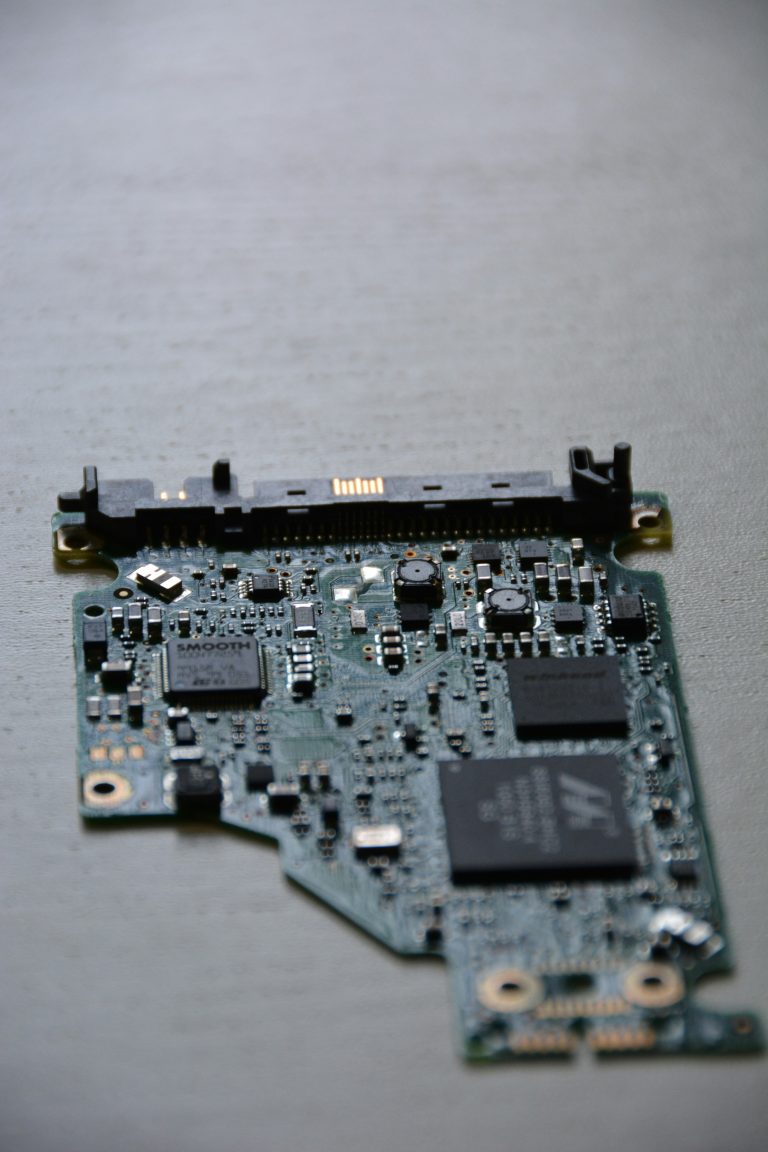
5. BGA Fanout Strategy & High-Speed Via Design
Reasonable BGA fanout design and via optimization are key difficulties in compact high-speed PCB layout. High-density chips widely adopt BGA packaging with compact pins and limited routing space.
5.1 BGA Fanout Solution by Pitch
| BGA Pitch | Fanout Method | Process Requirement |
|---|---|---|
| 1.0mm | Standard Through-Hole Fanout | Regular PCB process |
| 0.8mm | Through-Hole + Fine Trace | High-precision DFM inspection |
| 0.65mm | Blind & Mixed Via Fanout | Basic HDI technology |
| 0.5mm | Micro Blind Via | Laser microvia process |
| 0.4mm & below | Any-Layer HDI | High-end customized process |
5.2 Four Common High-Speed Via Types
- Through-Hole: Low cost, long stub, only suitable for medium and low speed.
- Blind Via: Short stub, excellent high-frequency performance.
- Buried Via: Hidden inside layers, perfect for multi-layer high-end boards.
- Microvia: Ultra-small hole for high-density BGA fanout.
5.3 Back-Drilling for Stub Removal
When the signal rate exceeds 3.125Gbps, redundant via stubs will cause resonance, signal attenuation and waveform distortion. Back-drilling is a necessary process for ultra-high-speed PCBs.
5.4 Via-in-Pad Design
- Resin-filled via: Smooth surface, stable high-frequency performance for high-speed signals.
- Copper-filled via: High current carrying capacity for power and ground nets.
6. Integrated Ground and Power Plane Design
Core Design Concept
Optimal PCB grounding design directly determines signal quality and electromagnetic performance. All high-frequency current must form a closed loop through the nearest complete reference plane.
6.1 Ground Plane Design Rules
- Use complete solid ground planes as much as possible.
- For mixed-signal products, separate analog and digital grounds with single-point grounding.
- Adopt unified complete ground for pure digital high-speed boards.
- Increase multi-layer ground to reduce overall impedance.
6.2 Power Plane Design Tips
- Independent complete plane for each voltage network.
- Power plane can be used as auxiliary AC reference.
- Place decoupling capacitors close to chip power pins.
6.3 Stitching Ground Vias
Arrange stitching vias between multi-layer grounds, high-speed via areas and board edges to suppress resonance and reduce interlayer impedance.
6.4 Ground Guard Trace Shielding
Add grounded guard traces for clock and sensitive signals to enhance shielding and anti-interference ability.
7. Clock Signal & Mainstream High-Speed Interface Layout
Professional high-speed interface layout directly affects transmission stability and long-term product reliability. Clock signals, as the main noise source, need priority protection in all high-speed projects.
7.1 Clock Signal Protection
- Follow the 3W spacing rule.
- Arrange clock traces on inner layers with full ground shielding.
- Minimize vias and layer switching.
- Keep away from high-current and switching power areas.
7.2 High-Speed Serial Interface
- Differential length tolerance within 5mil.
- AC coupling capacitors placed near the transmitter.
- Control via quantity and apply back-drilling for high-speed versions.
- Maintain 100Ω stable differential impedance.
7.3 High-Speed Memory Routing
| Signal Group | Length Control |
|---|---|
| DQ/DQS Data | ≤ 5mil in single byte group |
| Address & Command | ≤ 50mil relative to clock |
| Differential Clock | ≤ 2mil inner-pair tolerance |
7.4 High-Speed USB Interface
- 90Ω fixed differential impedance.
- Strict length matching and stable spacing.
- Isolate high-speed and low-speed signal areas.
8. High-Speed PCB DFM Rules & DRC Inspection
Standardized PCB DFM guidelines ensure high-speed designs match actual production technology, stabilizing mass production yield and controlling manufacturing costs.
- Reasonable trace width and spacing selection.
- Standard via size, aperture and annular ring design.
- Standardized solder mask and silkscreen layout.
- Complete DRC and DFM final inspection before production.
9. Comprehensive Design Summary
- Symmetric and reasonable PCB stackup design is the primary foundation of high-speed PCB design.
- Precise PCB impedance control must run through the whole design process.
- Standard differential pair routing eliminates common-mode noise and EMI risks.
- Complete PCB grounding design guarantees stable signal integrity.
- Optimized via optimization and stub removal support ultra-high-speed transmission.
- Scientific high-speed interface layout adapts to various high-bandwidth protocols.
- Accurate length matching and BGA fanout design improve overall design reliability.
10. FAQ – Frequently Asked Questions
Q1: What counts as a high-speed PCB?
A1: It is not defined by frequency only. The key standard is signal rise time. If the rise time is less than 6 times trace propagation delay, the board requires strict impedance control and shielding design.
Q2: What is the most critical factor in high-speed PCB design?
A2: Reasonable stackup layout and complete ground return paths, which cover most signal integrity challenges.
Q3: Why is differential length matching essential?
A3: Uneven trace lengths cause phase deviation, noise and data errors; keep inner-pair tolerance between 2mil to 5mil.
Q4: What are the common high-speed PCB impedance values?
A4: 50Ω for single-ended, 90Ω / 100Ω for differential pairs, 75Ω for video signals.
Q5: Is it allowed to split ground planes in high-speed projects?
A5: Not recommended. Split ground destroys return loops and increases electromagnetic interference.
11. Professional PCB Design Support & Business Inquiry
High-speed PCB design involves complex theories, strict technical constraints and rich manufacturing experience. We provide one-stop customized services for global engineers and purchasing teams:
✅ Free DFM design review and signal integrity risk analysis
✅ Custom PCB stackup design and impedance parameter tuning
✅ Professional BGA fanout design and via optimization
✅ HDI, back-drilling and filled via special process solutions
✅ Fast prototyping, mass production and customized quotation
Contact our team today for one-on-one technical support and tailored high-speed PCB solutions for your project.