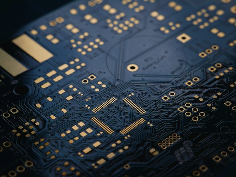
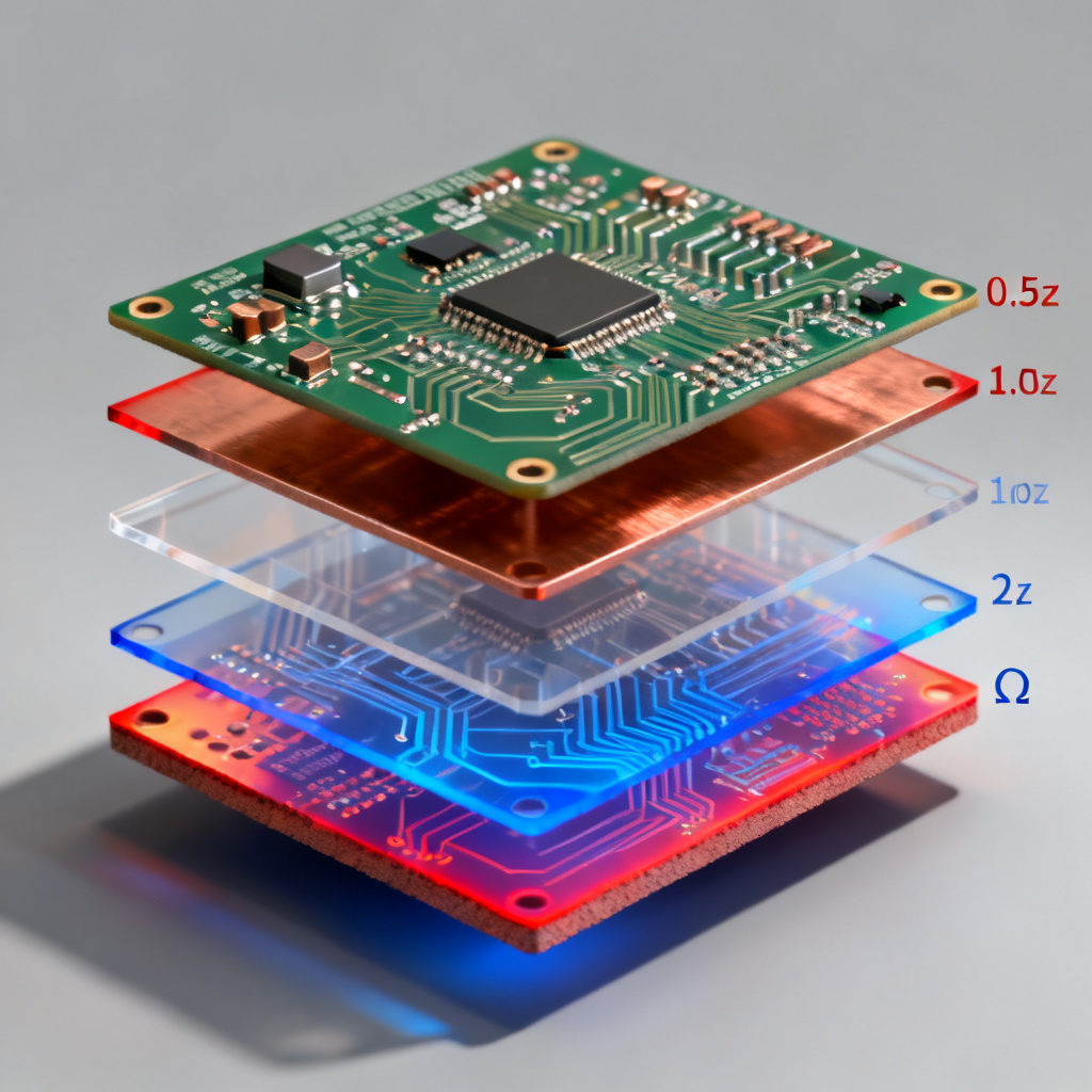
In high-speed PCB design, impedance control PCB performance depends on three core parameters: trace width (W), copper thickness (T), and dielectric height (H). These factors directly govern characteristic impedance, signal integrity, and manufacturing yield. Understanding their interplay is essential for achieving tight tolerances (±5% or ±10%) and reliable data transmission.
1. How Trace Width (W) Affects Impedance Control PCB
Trace Width and Characteristic Impedance Relationship
The most direct relationship in impedance control PCB design is that trace width is inversely proportional to characteristic impedance. As trace width increases, impedance decreases because a wider trace creates larger capacitance per unit length to the reference plane. For a microstrip line, the approximate formula is: Z0 = 87 / √(εr + 1.41) × ln(5.98H / (0.8W + T)). Here, W appears in the denominator, so a larger W reduces Z0, while a narrower trace increases impedance.
Practical Trade-offs for Trace Width
Trace width is the most commonly adjusted parameter during design because it is easiest to modify without changing the PCB stackup. However, very narrow traces (below 4 mils for outer layers) increase conductor losses and cause manufacturing difficulties like etching tolerance issues and open circuits. Very wide traces consume board real estate and can cause crosstalk in dense designs. For a standard 50Ω microstrip on FR-4 (Er ~4.2) with 1oz copper and 4 mil dielectric height, typical trace width is around 7–8 mils. Always use a field solver like Polar SI9000 for precise calculations.
2. How Copper Thickness (T) Affects Impedance Control PCB
Secondary but Critical Effect of Copper Thickness
Copper thickness (T) has a secondary but non-negligible effect on impedance control PCB performance. In the formula, T appears in the term (0.8W + T). An increase in copper thickness slightly reduces impedance because it increases the effective cross-sectional area of the conductor, thereby increasing capacitance. The effect is more pronounced for thin traces: for a 5-mil trace, increasing copper from 0.5oz to 2oz can reduce impedance by approximately 4–6Ω; for a 10-mil trace, the shift is only 2–3Ω.
Balancing Copper Thickness with Design Constraints
Copper thickness is often determined by current-carrying requirements (ampacity) and thermal management, not by impedance targets. Thicker copper lowers impedance, while thinner copper raises impedance. For high-speed signals, 1oz (1.4 mils) is the sweet spot for outer layers. Avoid 2oz or heavier copper for critical impedance-controlled traces unless absolutely necessary for power. If heavy copper is required, widen the trace to compensate for the impedance drop.
3. How Dielectric Height (H) Affects Impedance Control PCB
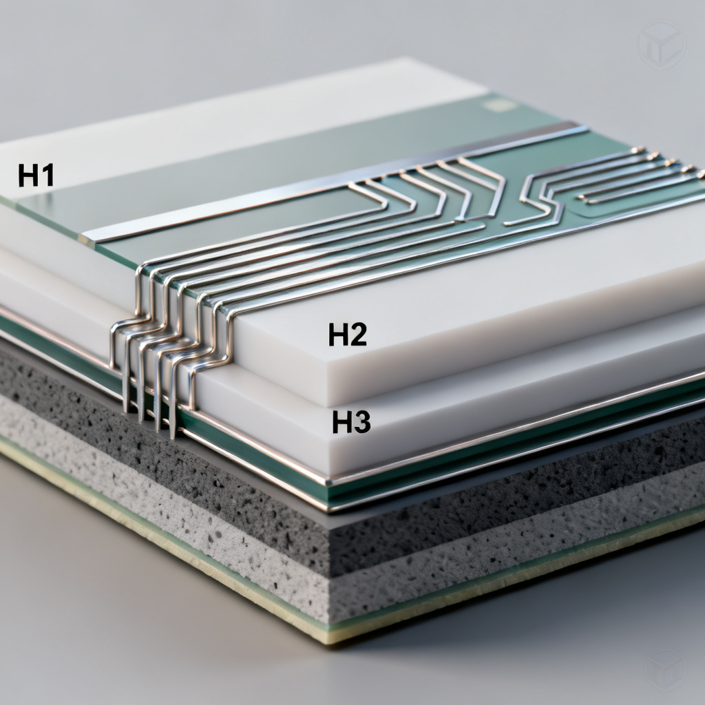
Dielectric Height as the Most Influential Parameter
Dielectric height (H) is the most influential single parameter for impedance control PCB design. In the microstrip formula, H appears in the numerator of the log term, so a larger H increases impedance by physically separating the trace from the reference plane, reducing capacitance. Doubling the dielectric height (e.g., from 4 mils to 8 mils) can increase impedance by approximately 10–15Ω for a given trace width, making H the primary tool for achieving high impedance values without resorting to extremely thin traces.
Manufacturing Constraints and Practical Rules
Dielectric height is determined by prepreg and core thicknesses in the PCB stackup. Thicker dielectrics require more material and longer press cycles, increasing cost. Thinner dielectrics (e.g., 2–3 mils) are common in HDI designs but are more prone to resin starvation and thickness variation. For a 50Ω microstrip with 1oz copper, a 4-mil dielectric height yields a trace width of ~7–8 mils. For a 100Ω differential pair, typical dielectric height is 4–6 mils with trace width of 4–5 mils and gap of 6–8 mils. Always consult your PCB manufacturer for preferred prepreg stackup options.
4. The Interplay of All Three Parameters in Impedance Control PCB Manufacturing
Impedance Tolerance Stacking
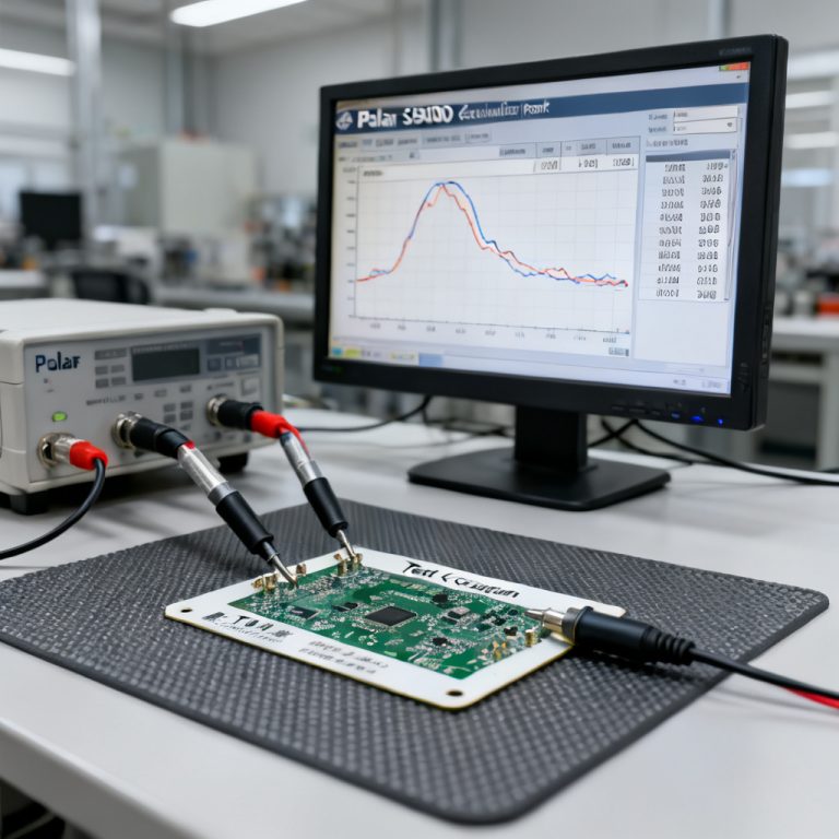
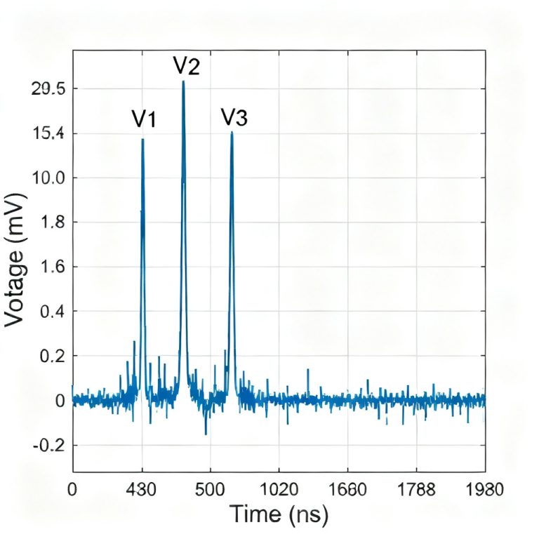
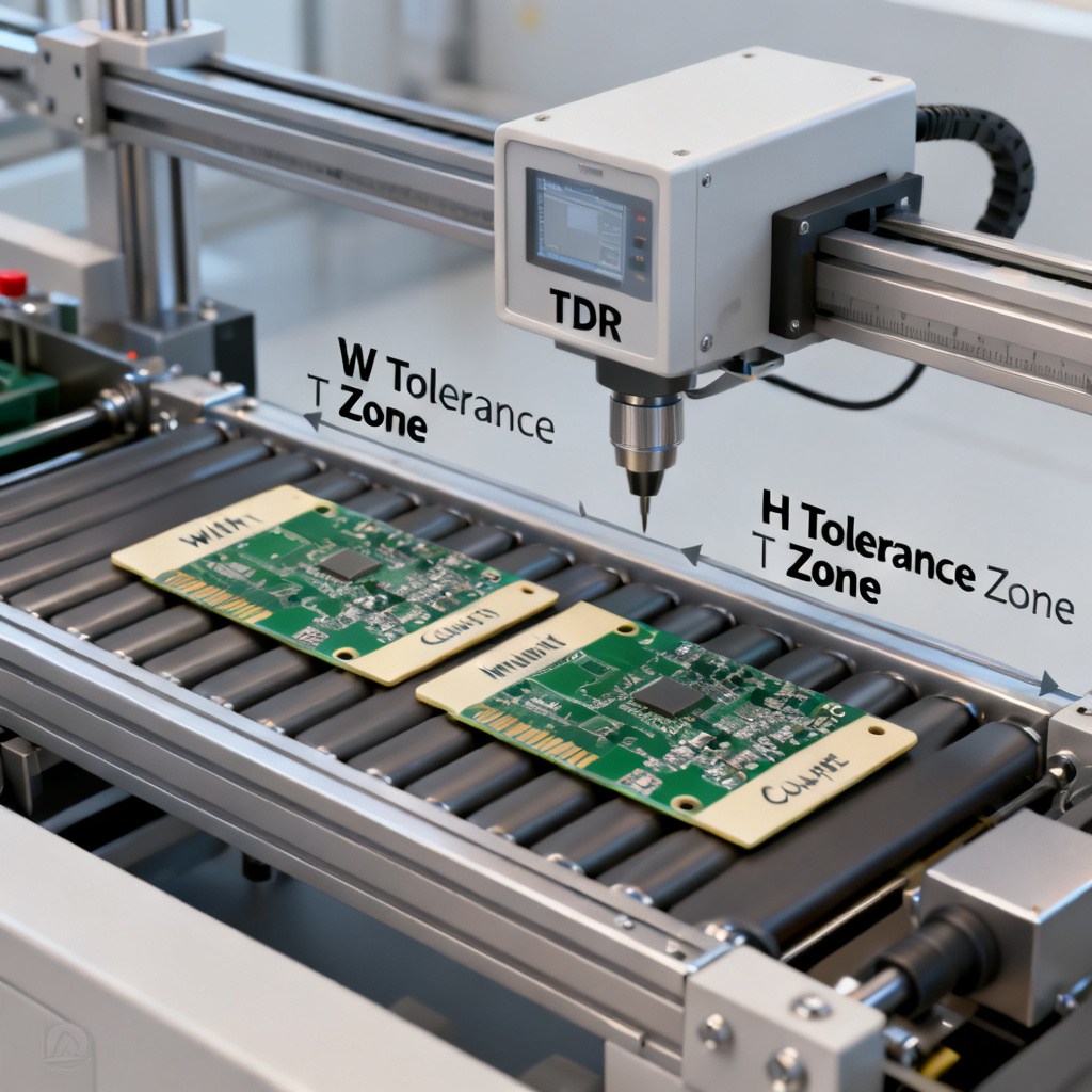
In real-world manufacturing, the three parameters are not independent. Etching tolerances affect trace width (W), copper plating variation affects thickness (T), and prepreg thickness variation with glass weave effect affects dielectric height (H). For a target of 50Ω ±10%, combined variation of ±10% in W, ±20% in T, and ±10% in H can easily push performance outside spec. This is why controlled impedance testing via Time Domain Reflectometry (TDR) is mandatory for high-speed designs.
Mitigation Strategies
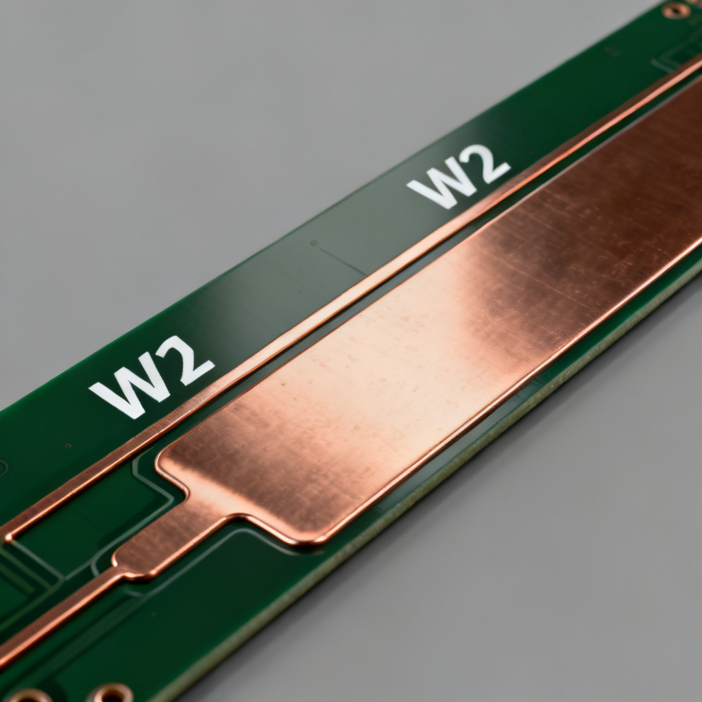
Designers often use impedance coupons on production panels—test structures that mimic actual traces. Manufacturers measure these coupons to verify that impedance meets the target after etching and plating. Successful impedance control PCB strategy must account for all three variables simultaneously.
| Parameter | Increase Effect on Impedance | Primary Constraint | Manufacturing Challenge |
|---|---|---|---|
| Trace Width (W) | Decreases | Layout density, conductor loss | Etching tolerance, fine-line capability |
| Copper Thickness (T) | Decreases (slightly) | Current capacity, thermal management | Plating uniformity, etch factor |
| Dielectric Height (H) | Increases | Board thickness, cost, via aspect ratio | Prepreg thickness variation, glass weave |
5. Advanced Considerations for High-Speed Impedance Control PCB Design
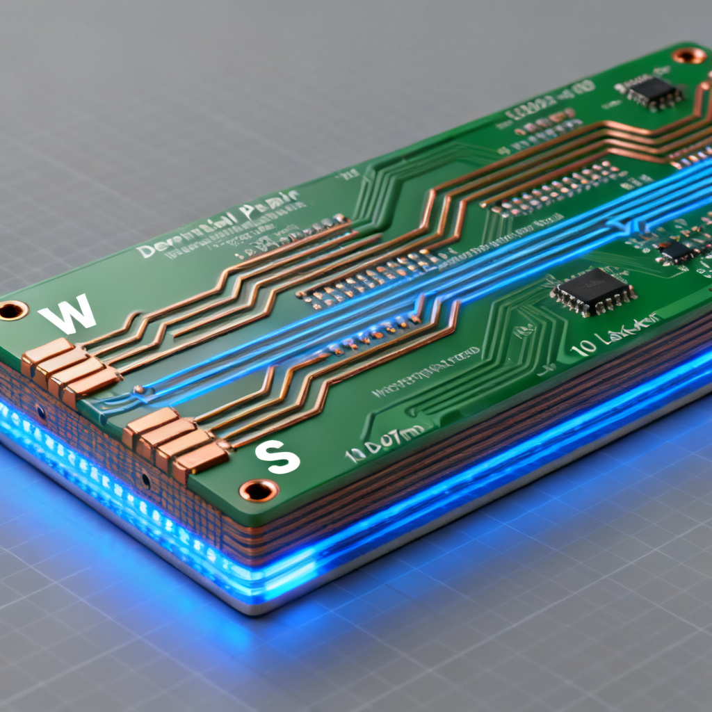
Differential Impedance and Solder Mask Effects
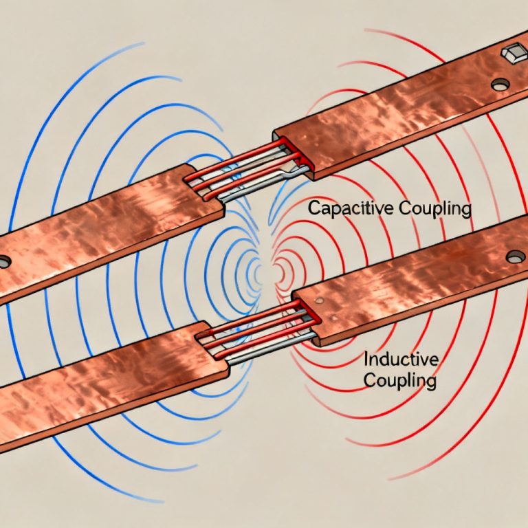
For differential pairs (e.g., USB, HDMI, PCIe), trace width (W), trace spacing (S), and dielectric height (H) all affect odd-mode impedance. Wider spacing increases differential impedance (reduces coupling), while tighter spacing decreases it. Solder mask also impacts impedance control PCB performance: it has a dielectric constant (Er ~3.5–4.0) and thickness of 0.5–1.0 mil, effectively reducing microstrip impedance by 2–4Ω. Always account for solder mask in calculations, especially for fine-pitch traces.
Material Selection and Reference Plane Integrity
FR-4 has a wide tolerance on dielectric constant (Er = 4.2 ± 0.2). For designs above 1 Gbps, use low-loss, stable materials like Rogers, Isola, or high-end FR-4 variants (e.g., IT-180A, Nelco 4000-13) that offer tighter Er control and lower dissipation factor (Df). The reference plane (ground or power) must be continuous directly under the trace; any gaps, slots, or splits cause sudden impedance increases (impedance discontinuity), leading to reflections and signal degradation.
Industry Terminology Explained
Characteristic impedance: The constant impedance a transmission line exhibits for a signal traveling along it, typically 50Ω or 100Ω differential. Dielectric constant (Er): The material’s ability to store electrical energy, affecting signal velocity and impedance. Dissipation factor (Df): A measure of signal loss in the dielectric material. Time Domain Reflectometry (TDR): A measurement technique used to verify impedance by sending a fast pulse and analyzing reflections.
Frequently Asked Questions About Impedance Control PCB
What is the most important parameter for impedance control PCB?
Dielectric height (H) is the most influential parameter for impedance control PCB design, as it directly and significantly affects characteristic impedance. However, all three parameters—trace width, copper thickness, and dielectric height—must be balanced for optimal performance.
How does copper thickness affect impedance control PCB?
Copper thickness (T) has a secondary effect: thicker copper slightly reduces impedance, while thinner copper increases it. This is critical for impedance control PCB designs where current-carrying requirements conflict with impedance targets.
Can I use FR-4 for high-speed impedance control PCB?
FR-4 is suitable for impedance control PCB designs up to about 1 Gbps, but for higher speeds, low-loss materials with tighter Er control (e.g., Rogers, Isola) are recommended to maintain signal integrity.
Why is trace width inversely proportional to impedance?
Wider traces increase capacitance per unit length to the reference plane, lowering characteristic impedance. This inverse relationship is fundamental to impedance control PCB design and is captured in the microstrip impedance formula.
To achieve precision in impedance control PCB manufacturing, collaborate closely with your PCB manufacturer. Provide a detailed stackup with specified impedance targets, preferred trace widths, and acceptable tolerances. Use field solvers for pre-layout calculations and TDR testing for post-production verification. By mastering these three critical parameters, you can design PCBs that deliver reliable, high-speed performance with minimal signal integrity issues.
Need a prototype or production run for your high-speed impedance control PCB? Contact our engineering team today for a free stackup review and impedance calculation. We specialize in tight-tolerance, high-yield manufacturing for B2B clients worldwide.
“`