Generating a crosstalk report for high speed PCB design review is essential to ensure signal integrity and avoid costly redesigns. This guide covers the complete process.
In high-speed PCB design, crosstalk—the unwanted coupling of signals between adjacent traces—can lead to timing violations, data corruption, and system failures. Generating a comprehensive crosstalk report during the design review phase is critical for identifying and mitigating these issues before fabrication. This pillar content guides you through the entire process, from understanding fundamental coupling mechanisms to running simulations and interpreting results. By leveraging insights from industry-leading sources, we provide a step-by-step approach to create a reliable crosstalk report that ensures your high-speed PCB meets signal integrity (SI) standards.
Understanding Crosstalk in High Speed PCB Design
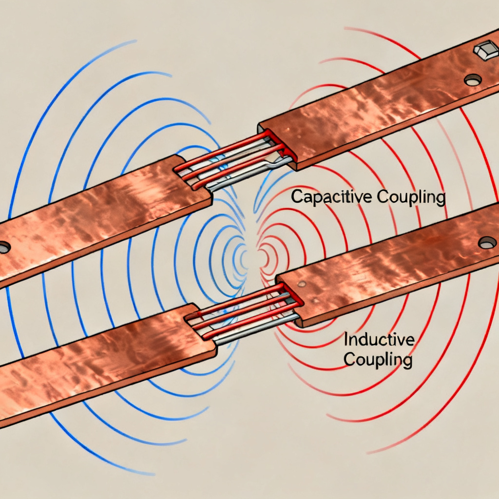
Understanding crosstalk in high speed PCB design begins with the two primary coupling mechanisms: capacitive (electric field) and inductive (magnetic field).
Capacitive and Inductive Coupling
Crosstalk occurs when electromagnetic fields from one signal trace (the aggressor) induce unwanted voltage or current in a neighboring trace (the victim). Capacitive coupling is dominant when traces are in close proximity and high-frequency signals create a parasitic capacitance between them. Inductive coupling arises from mutual inductance between parallel traces, where current changes in the aggressor induce a voltage in the victim. This is more significant at higher frequencies and in longer parallel runs.
Forward and Backward Crosstalk
Crosstalk manifests in two forms: forward crosstalk, which propagates in the same direction as the aggressor signal, and backward crosstalk, which travels opposite to the aggressor signal. In microstrip lines, backward crosstalk is usually larger and has a longer duration, proportional to the coupling length. For stripline, backward crosstalk can be minimized with proper stack-up design.
Key Parameters Influencing Crosstalk
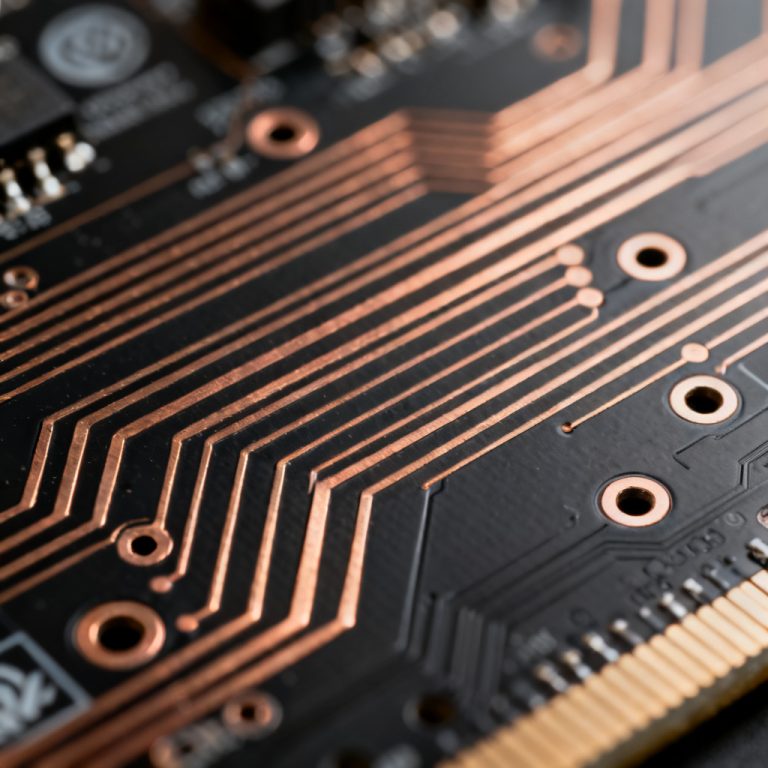
Key parameters influencing crosstalk include trace spacing, dielectric height, rise time, parallel run length, and termination. A common guideline is the 3W rule, but this may not suffice for GHz-range signals.
Preparing for Crosstalk Simulation for High Speed PCB Design Review
Preparing for crosstalk simulation for high speed PCB design review requires defining the stack-up, extracting net topology, and configuring simulation parameters.
Define the PCB Stack-Up
Accurate crosstalk analysis requires a precise stack-up model. Key details include layer count and order, material properties (dielectric constant and loss tangent), copper thickness and roughness, and impedance targets.
Extract the Net Topology
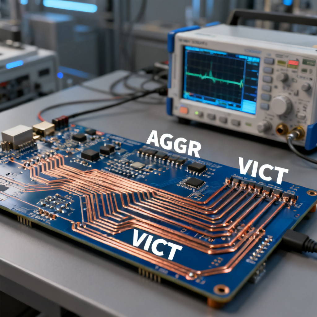
Select the nets of interest, typically high-speed signals like clocks, data buses (DDR, PCIe, USB), and sensitive analog traces. Use a 2D or 3D field solver to extract transmission line parameters and mutual coupling parameters.
Set Simulation Conditions
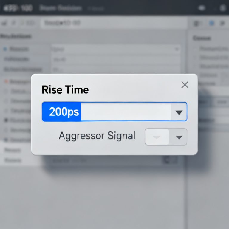
Define the aggressor signal characteristics, including signal type, rise time, source and load models, and frequency range.
Step-by-Step Guide to Generate a Crosstalk Report for High Speed PCB Design Review
This step-by-step guide to generate a crosstalk report for high speed PCB design review covers setting up the simulation environment, configuring the simulation, running it, analyzing results, and generating the report.
Step 1: Set Up the Simulation Environment
Import the PCB layout, select nets (aggressor and victim), and define the simulation type as “Coupling Analysis” or “Crosstalk Simulation.”
Step 2: Configure the Crosstalk Simulation
Assign IBIS or SPICE models to drivers and receivers. Apply a step or pulse to the aggressor net. Define probes at near end and far end of both nets. Specify sweep parameters if needed.
Step 3: Run the Simulation
Execute the transient analysis. Monitor convergence and adjust solver settings if necessary.
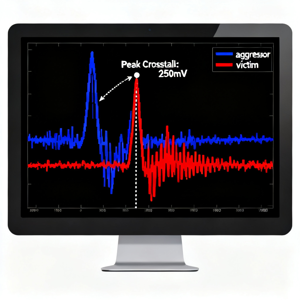
Step 4: Analyze the Results
View waveforms and calculate peak crosstalk voltage, crosstalk duration, and crosstalk coefficient. Apply mask limits to check for logic errors.
Step 5: Generate the Crosstalk Report
Document parameters, present waveforms, tabulate results, include recommendations, and export the report as PDF or HTML.
| Victim Net | Coupling Length (in) | Spacing (mils) | NEXT (mV) | FEXT (mV) | Pass/Fail |
|---|---|---|---|---|---|
| DATA_CLK | 2.5 | 5 | 85 | 12 | Fail |
| ADDR_BUS | 1.8 | 8 | 45 | 8 | Pass |
Best Practices for Crosstalk Mitigation in High Speed PCB Design
Best practices for crosstalk mitigation in high speed PCB design include adhering to the 3W rule, using guard traces, optimizing stack-up, minimizing parallel runs, controlling rise time, and terminating properly.
Adhere to the 3W Rule
For most high-speed designs, maintain trace spacing equal to three times the trace width. For critical signals like clocks, use 5W or 10W.
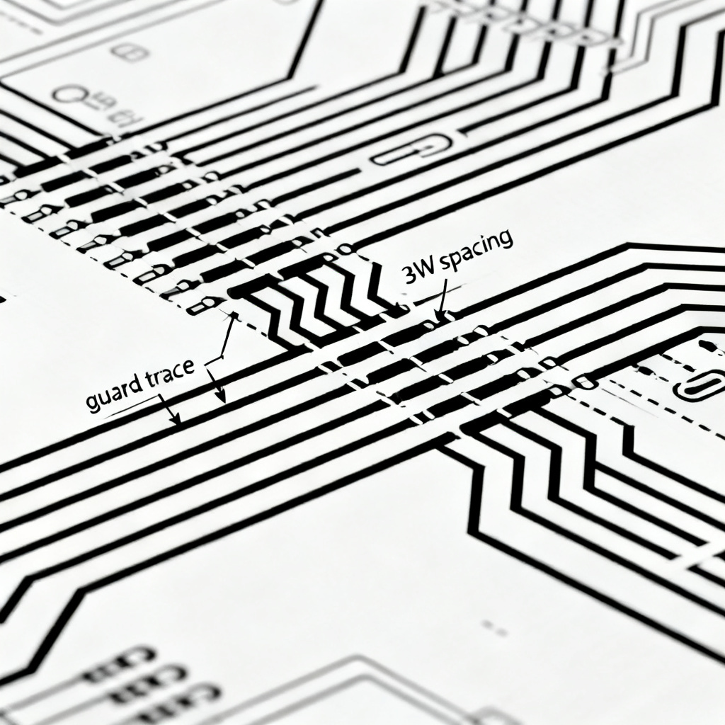
Use Guard Traces
Place a grounded copper trace between aggressor and victim nets, spaced at least 2W from each trace, and stitch it to the ground plane with vias every λ/10.
Optimize Stack-Up
Use thin dielectrics between signal and reference planes. Place high-speed signals on inner layers (stripline) to reduce radiation and far-end crosstalk.
Minimize Parallel Runs
Route critical signals orthogonally on adjacent layers. If parallel runs are unavoidable, keep them under 1 inch.
Control Rise Time
Use drivers with slower rise times if timing margins allow. A 500 ps rise time generates less crosstalk than a 100 ps rise time.
Terminate Properly
Use series termination at the source to dampen reflections and reduce the aggressor’s voltage swing.
Common Pitfalls in High Speed PCB Crosstalk Analysis
Common pitfalls in high speed PCB crosstalk analysis include ignoring via coupling, overlooking power integrity, using inaccurate models, assuming symmetry, and failing to validate.
Ignoring Via Coupling
Vias can act as antennas. Simulate via crosstalk for dense designs and use ground vias adjacent to signal vias.
Overlooking Power Integrity
Noise on power planes can couple into signals. Ensure decoupling capacitors are placed near high-speed ICs.
Using Inaccurate Models
Always use vendor-supplied IBIS models instead of generic libraries.
Assuming Symmetry
Differential pairs must have equal lengths and spacing to avoid mode conversion and crosstalk.
Failing to Validate
Verify simulation results with measurements on a prototype using a time-domain reflectometer (TDR).
Advanced Considerations for High Speed PCB Crosstalk
Advanced considerations for high speed PCB crosstalk include frequency-dependent coupling, 3D full-wave simulation, statistical analysis, and crosstalk induced jitter conversion.
Frequency-Dependent Coupling
Use S-parameter extraction to model crosstalk across a frequency range, essential for serial links like PCIe Gen 4/5 or 10G Ethernet.
3D Full-Wave Simulation
For complex structures like BGA breakout regions or connectors, use 3D solvers like Ansys HFSS.
Statistical Analysis
Run Monte Carlo simulations with manufacturing tolerances to ensure robustness.
Crosstalk Induced Jitter
Convert crosstalk voltage to timing jitter using the signal slew rate. For example, a 50 mV crosstalk on a 1V/ns signal adds 50 ps of jitter.
Frequently Asked Questions About Crosstalk Report for High Speed PCB Design Review
What is a crosstalk report for high speed PCB design review?
A crosstalk report for high speed PCB design review is a document that captures simulation results, parameters, and recommendations to ensure signal integrity by minimizing unwanted coupling between traces.
How do you generate a crosstalk report for high speed PCB design review?
To generate a crosstalk report for high speed PCB design review, define the stack-up, extract net topology, configure simulation parameters, run the simulation, analyze waveforms, and document results with tables and recommendations.
What are the key parameters in a crosstalk report for high speed PCB design review?
Key parameters include trace spacing, coupling length, rise time, dielectric height, and termination. These are documented in the crosstalk report for high speed PCB design review.
How can crosstalk be reduced in high speed PCB design?
Crosstalk can be reduced by increasing trace spacing, adding guard traces, using stripline layers, minimizing parallel runs, and controlling rise time, as detailed in the crosstalk report for high speed PCB design review.
Conclusion
Generating a crosstalk report for high speed PCB design review is a vital step in ensuring signal integrity and system reliability. By following the structured workflow outlined in this guide—preparing the stack-up, running simulations, analyzing results, and implementing mitigations—you can identify and resolve coupling issues early in the design cycle. Remember to document all parameters and recommendations in a clear, actionable report. With practice, you will master the art of crosstalk analysis, enabling your high-speed PCB designs to perform flawlessly in the most demanding applications.
Need expert assistance with your high-speed PCB design? Contact our team for professional design review and crosstalk analysis. We specialize in custom PCB fabrication and assembly for high-speed applications, ensuring your product meets the highest signal integrity standards. Request a quote today.