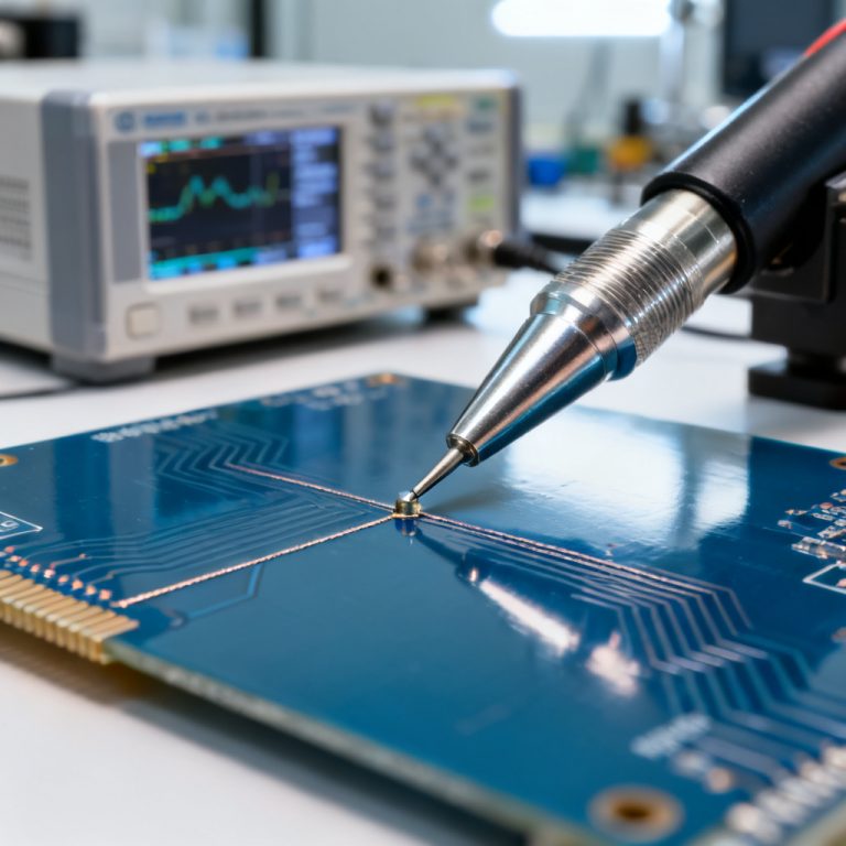
Mastering oscilloscope calibration for accurate eye diagram PCB results is the foundation of high-speed signal integrity analysis. Without precise calibration, your eye diagrams may misrepresent jitter, noise, or timing errors, leading to costly design iterations. This guide synthesizes best practices from leading industry sources to deliver a complete, step-by-step approach to oscilloscope calibration for eye diagram analysis in high-speed PCB design.
Understanding the Calibration Chain for Eye Diagram PCB Results
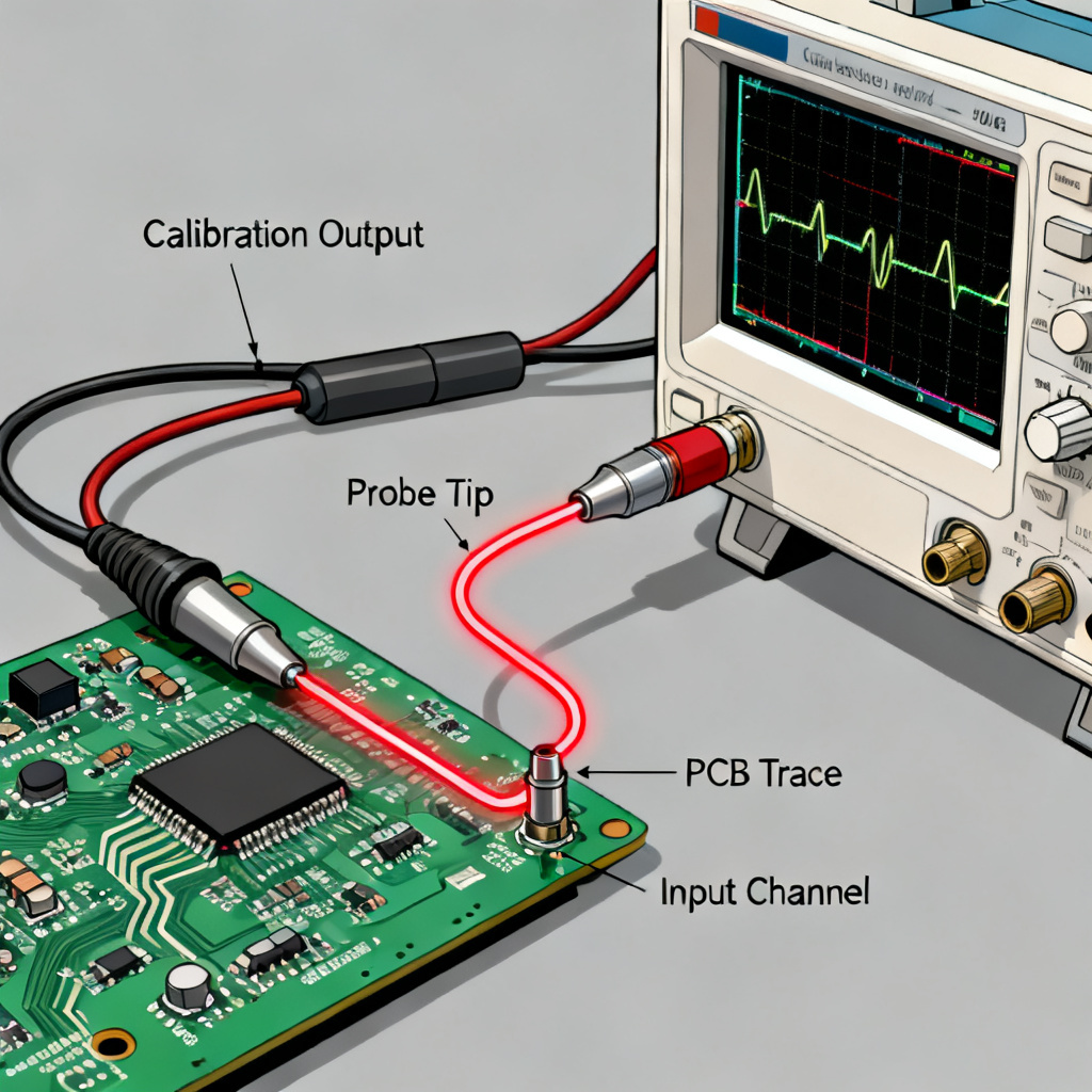
Before diving into procedures, you must understand the entire signal path that affects your eye diagram. Oscilloscope calibration for accurate eye diagram PCB results is not a single action; it is a chain of corrections applied to the oscilloscope, probes, cables, and fixtures.
The Signal Path Components
- Oscilloscope Front-End: Includes the amplifier, attenuator, and digitizer. Internal calibration corrects for DC offset, gain error, and bandwidth limitations.
- Probes: Active or passive probes have their own frequency response, attenuation, and delay. Probe compensation matches the probe to the oscilloscope input.
- Cables and Connectors: Coaxial cables and adapters introduce loss, reflections, and skew. De-embedding removes these effects mathematically.
- Test Fixtures: For PCB testing, fixtures (e.g., SMA connectors, differential probes) add parasitics that must be characterized.
The Role of De-Embedding
De-embedding is a calibration technique that mathematically removes the effects of the test fixture and cables from the measurement. For eye diagrams, this is critical because the fixture’s impedance discontinuities can distort the signal. Using S-parameter models of your fixture (obtained through VNA measurements or simulation), the oscilloscope can reconstruct the actual signal at the DUT (Device Under Test) pins.
Why Calibration Prevents False Eye Diagram Failures
A poorly calibrated system can make a clean signal appear to have excessive jitter or a closed eye. Conversely, it can hide real issues like crosstalk or reflections. Industry standards (e.g., IEEE 802.3, JEDEC) require specific calibration procedures to ensure compliance testing passes or fails correctly.
Step-by-Step Oscilloscope Calibration for Accurate Eye Diagram PCB Results
This section combines the most practical, actionable steps for oscilloscope calibration for accurate eye diagram PCB results from the top-ranking sources. Perform these steps in order for every measurement session.
Step 2.1: Warm-Up and Self-Calibration
- Power on the oscilloscope and allow 30-60 minutes for thermal stabilization. Internal components drift with temperature; warm-up ensures accuracy.
- Run the oscilloscope’s built-in self-calibration routine. Most modern scopes (e.g., Keysight, Tektronix, LeCroy) have an internal calibration signal. Access this via the Utilities or Calibration menu. This corrects for DC offsets, gain, and timebase errors.
- Check the calibration status. Verify the “Calibration Due” date is not expired. If expired, send the scope to a certified calibration lab.
Step 2.2: Probe Compensation and Deskew
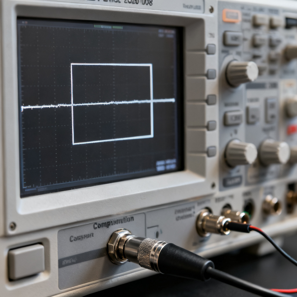
- Probe Compensation (Low-Frequency): Attach the probe to the scope’s 1 kHz square wave output. Adjust the probe’s compensation trimmer (usually a small screw) until the displayed square wave has flat tops and sharp corners, without overshoot or rounding. This matches the probe’s capacitance to the scope input.
- Probe Deskew (High-Frequency): For differential or multi-channel measurements (common in eye diagrams), deskew is essential. Use a known low-jitter reference signal (e.g., a clock source) connected to all channels with identical cables. Adjust the deskew settings in the oscilloscope menu so that the rising edges align within a few picoseconds. This eliminates timing skew that would artificially widen the eye’s horizontal opening.
- Active Probe Calibration: If using active probes (e.g., for high-impedance measurements), perform the probe’s own zero-offset and gain calibration using the probe’s dedicated calibration fixture (often a shorted or open circuit).
Step 2.3: Timebase and Trigger Calibration
- Timebase Calibration: Use the oscilloscope’s built-in time mark generator (if available) or an external time reference (e.g., a GPS-disciplined oscillator) to verify timebase accuracy. For eye diagrams, a 1-2% timebase error can cause significant jitter measurement errors.
- Trigger Calibration: Set the trigger to the data rate of your PCB signal (e.g., 10.3125 Gbps for 10GbE). Use a clean clock signal to verify the trigger threshold is accurate. A miscalibrated trigger can cause the eye diagram to shift horizontally, making the eye appear closed.
Step 2.4: De-Embedding and Fixture Calibration
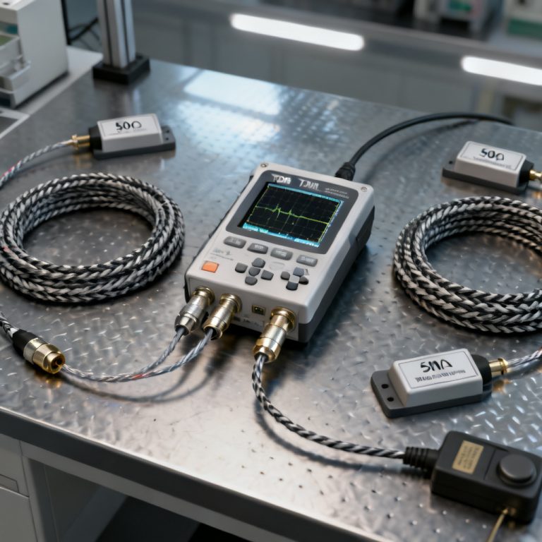
- Characterize the Test Fixture: Measure the S-parameters of your PCB test fixture (including cables and connectors) using a Vector Network Analyzer (VNA) up to at least 3x the signal bandwidth. Save the S4P or S2P file.
- Load S-Parameters into the Oscilloscope: Most high-end scopes (e.g., Keysight Infiniium, Tektronix DPO70000) support de-embedding. Load the fixture’s S-parameter file and apply de-embedding to the measurement channel(s). The scope will mathematically remove the fixture’s effects.
- Verify De-Embedding: After applying de-embedding, measure a known clean signal (e.g., a short through line) to confirm the eye diagram now matches the expected shape. If the eye still shows anomalies, check the fixture’s S-parameter quality.
Step 2.5: Noise and Jitter Floor Verification
- Measure the Oscilloscope’s Own Noise: Set the input to 50Ω termination (or probe connected but not touching any signal). Capture a noise floor trace. For accurate eye diagrams, the scope’s noise should be at least 6 dB below your signal’s noise floor. If not, consider using low-noise probes or averaging.
- Measure Jitter Floor: Use a precision clock source (e.g., a signal generator with <1 ps RMS jitter) as the input. The measured jitter from the oscilloscope should be within its specifications (typically <1 ps RMS for high-end scopes). If jitter is higher, check for ground loops or power supply noise.
Advanced Calibration Techniques for High-Speed PCBs
For B2B applications where signal integrity is paramount (e.g., 25 Gbps+ designs), standard oscilloscope calibration for accurate eye diagram PCB results may not suffice. These advanced steps are derived from expert sources.
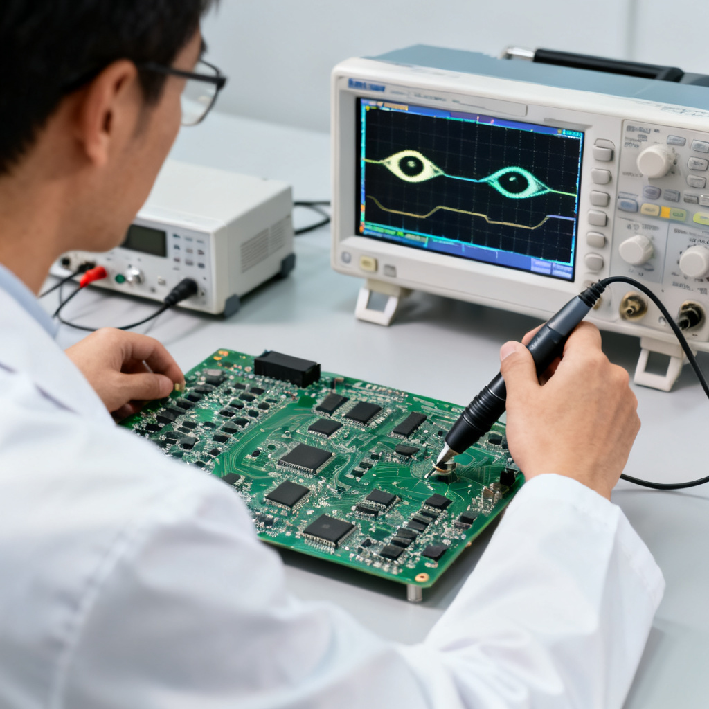
Differential Calibration
- Most high-speed PCB signals are differential (e.g., LVDS, CML). Use differential probes or two matched single-ended probes with a differential de-embedding setup.
- Calibrate both channels for gain and skew simultaneously. Apply a differential de-embedding file that accounts for the pair’s common-mode and differential-mode S-parameters.
- Verify differential eye diagrams by measuring a known differential clock. The eye should be symmetric with zero common-mode offset.
Calibration for DDR Memory Interfaces
- DDR signals (e.g., DDR4, DDR5) require read/write separation. Calibrate the oscilloscope to trigger on specific DDR commands (e.g., READ burst using a protocol decoder).
- Use the oscilloscope’s DDR-specific calibration wizard, which often includes DQ/DQS deskew and Vref calibration. This ensures the eye diagram captures the actual data valid window.
Temperature and Environmental Calibration
- High-speed PCB testing often occurs in controlled environments. However, if your lab temperature fluctuates, perform calibration at the same temperature as the measurement.
- For production testing, consider automated calibration scripts that re-run self-calibration every hour to compensate for drift.
Calibration of Eye Mask Testing
- If your eye diagram includes a compliance mask (e.g., PCIe Gen 4 mask), calibrate the mask’s position and voltage levels. Use a known good signal to verify the mask margins.
- Ensure the oscilloscope’s mask margin calculation accounts for the calibration-induced uncertainty. Most scopes provide a “measurement uncertainty” report.
Common Calibration Mistakes and How to Avoid Them
Even experienced engineers make errors. Here are the most frequent pitfalls in oscilloscope calibration for accurate eye diagram PCB results, based on industry feedback.
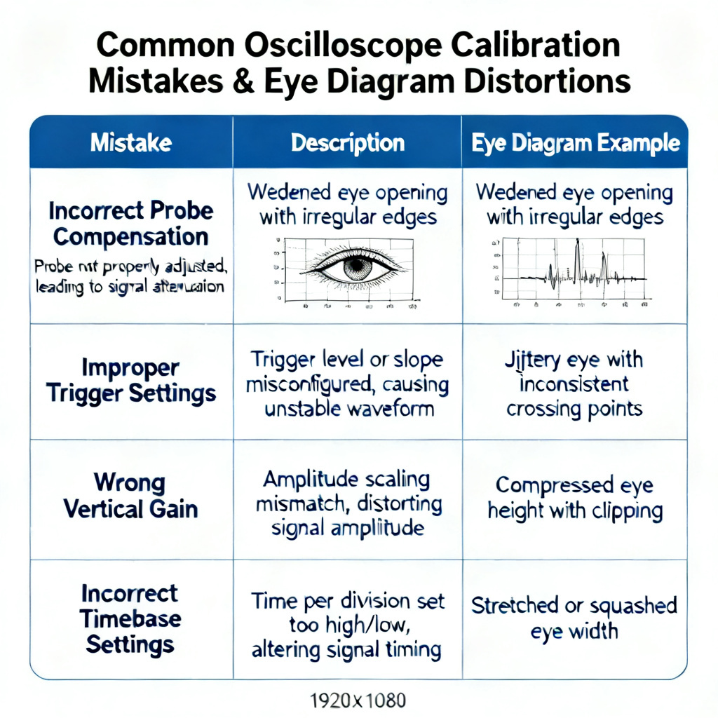
| Calibration Mistake | Impact on Eye Diagram PCB Results | Solution |
|---|---|---|
| Skipping Probe Compensation | Overshoot or rounding in the eye diagram, leading to false mask violations | Always perform probe compensation before any eye diagram measurement. Use the scope’s internal 1 kHz square wave. |
| Ignoring Cable Loss | The eye diagram appears closed due to high-frequency attenuation from long cables | Use short, high-quality cables (e.g., 1 meter maximum for 10 Gbps). Apply de-embedding if cables are longer. |
| Using Incorrect Termination | Reflections cause eye diagram ghosting or double edges | Ensure the oscilloscope input impedance matches the PCB trace impedance (typically 50Ω single-ended, 100Ω differential). |
| Not Re-Calibrating After Changing Probes | Skew and gain errors from different probes corrupt the measurement | Re-run deskew and compensation every time you change a probe or cable. |
| Overlooking Ground Loops | Excessive low-frequency noise in the eye diagram | Use a single-point ground connection between the PCB, probe, and oscilloscope. Use isolation transformers if necessary. |
Validating Your Calibration with a Reference Signal
Before trusting your eye diagram results, validate the entire calibration chain for oscilloscope calibration for accurate eye diagram PCB results.
The Golden Device Method
- Keep a known-good PCB (e.g., a simple PRBS pattern generator) with well-characterized output. Measure its eye diagram immediately after calibration.
- Compare the measured eye height, width, and jitter to the known values (from a trusted lab). If they match within 5%, your calibration is acceptable.
Use Built-in Validation Tools
- Many oscilloscopes have a “Calibration Check” mode that compares measurements against internal standards. Run this after every calibration.
- For eye diagrams, look for the “Eye Diagram Quality Indicator” (e.g., Keysight’s EZJIT) that flags if the measurement is likely affected by calibration errors.
Document Your Calibration
- For B2B compliance (e.g., ISO 9001), maintain a calibration log. Record date, time, temperature, scope serial number, and any de-embedding files used. This ensures traceability for customer audits.
FAQ: Oscilloscope Calibration for Eye Diagram PCB Results
What is the most important step in oscilloscope calibration for accurate eye diagram PCB results?
The most critical step is performing probe compensation and deskew, as these directly affect the timing and amplitude accuracy of the eye diagram. Without proper deskew, the eye’s horizontal opening may be artificially narrowed.
How often should I perform oscilloscope calibration for eye diagram PCB results?
For production testing, calibrate at the start of each session and after any change in probes or cables. For R&D, a full calibration chain (including de-embedding) should be performed at least daily or whenever the test environment changes.
Can I use built-in oscilloscope calibration for accurate eye diagram PCB results without external references?
Built-in self-calibration corrects for internal errors but does not account for probe, cable, or fixture effects. For accurate eye diagrams, always supplement self-calibration with external deskew, compensation, and de-embedding.
What is the role of de-embedding in oscilloscope calibration for accurate eye diagram PCB results?
De-embedding removes the electrical effects of test fixtures and cables from the measurement, allowing you to see the true signal at the PCB pins. This is essential for high-speed signals above 1 Gbps where fixture parasitics dominate.
How do I verify my oscilloscope calibration for accurate eye diagram PCB results?
Use the Golden Device Method: measure a known-good PCB with a well-characterized eye diagram. If your measured eye height, width, and jitter match the known values within 5%, your calibration is valid.
In the high-speed PCB industry, delivering accurate eye diagram results is a hallmark of technical expertise. Proper oscilloscope calibration for accurate eye diagram PCB results not only ensures your designs meet specifications but also builds trust with clients who rely on your measurement data. By following this comprehensive calibration guide—from warm-up and probe compensation to advanced de-embedding and environmental control—you can produce eye diagrams that are repeatable, accurate, and compliant with industry standards. For your B2B customers, this means fewer design iterations, faster time-to-market, and confidence in your PCB fabrication and assembly services. Remember: A well-calibrated oscilloscope is the foundation of signal integrity. Invest the time, and your eye diagrams will never lie.
Call to Action: Need high-speed PCBs with guaranteed signal integrity? Contact our engineering team for a free design review and calibration consultation. We specialize in High Speed PCB fabrication up to 50 Gbps with full eye diagram testing support.