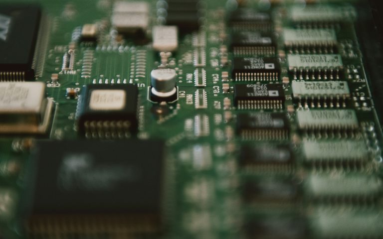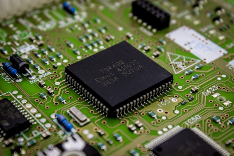
High-Speed PCB Via Design Guide: Stub Effect, Back Drilling & Impedance Optimization
Vias are the most critical and uncontrollable part of high-speed PCB signal paths. Acting as a combination of parasitic capacitance, inductance, and redundant stub segments, poorly designed vias cause signal attenuation, resonance, jitter, and impedance discontinuity—especially for 10Gbps+, 25Gbps SerDes, PCIe, and DDR high-speed applications. Mastering high speed PCB via design is essential for every…