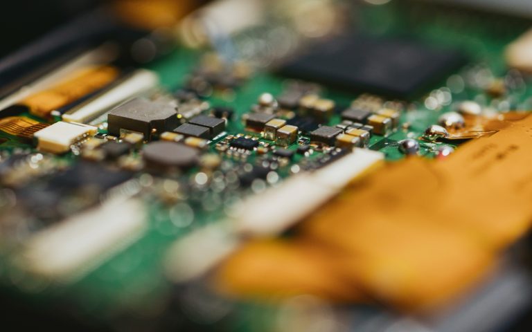
In high-speed PCB design, grounding is always the most underestimated yet critical design step. Most designers still regard ground as a simple 0V DC reference point, but high-frequency circuits require a completely different mindset: ground is a low-impedance continuous signal return path. As covered in our PCB Design Guidelines, mastering PCB grounding techniques is essential for signal integrity and EMC compliance.
This pillar guide integrates authoritative design practices from Cadence, Analog Devices and professional PCB industry resources. It simplifies professional theories while retaining engineering depth, covering grounding principles, solid ground plane design, split ground application rules, stitching via layout, mixed-signal grounding strategy, chassis ground connection, design checklist and common FAQ. Implementing proper PCB grounding techniques directly impacts your board’s signal quality and certification success.
Table of Contents
- 1. Why Grounding Matters in High-Speed PCB Design
- 2. Ground Is Not Only 0V — It’s a High-Speed Return Path
- 3. Solid Ground Plane: The Gold Standard for High-Speed PCBs
- 4. Split Ground Planes: Allowed Scenarios & Strict Design Rules
- 5. Stitching Vias and Ground Grids: Layout Rules & Spacing Guidelines
- 6. Mixed-Signal Grounding: AGND vs DGND Best Practice
- 7. Chassis Ground and PCB Signal Ground Connection Methods
- 8. High-Speed PCB Grounding Design Checklist
- 9. Core Key Takeaways
- 10. FAQ on High-Speed PCB Grounding
- 11. Professional Grounding Design Review & Quotation
Why Grounding Matters in High-Speed PCB Design
Grounding is the foundation of high-speed PCB signal integrity, power integrity and EMI/EMC performance. Many beginners mistakenly believe good grounding only needs low DC resistance, but high-speed circuits operate at high frequency where AC impedance, return path continuity and signal loop area dominate overall performance. Understanding PCB grounding techniques is the first step toward reliable high-speed design.
Poor grounding will directly cause a series of engineering problems: signal jitter, crosstalk distortion, power rail noise, plane resonance, electromagnetic radiation over-limit and EMC certification failure. For industrial control, automotive, 5G communication and high-speed digital products, standardized PCB grounding techniques are indispensable to ensure long-term stable operation of the whole system. Good high-speed grounding is not just wiring to GND pins; it is systematic layout planning that controls noise radiation and optimizes signal transmission quality from the source.
Ground Is Not Only 0V — It’s a High-Speed Return Path
Traditional low-frequency design treats ground merely as a fixed 0V reference potential for circuit biasing and DC power supply. Under low-frequency conditions, signal current only cares about power supply loop and DC reference, and return path is often ignored in layout. This is one of the most common misconceptions that proper PCB grounding techniques must correct.
However, high-frequency working principles are completely different. Every high-speed alternating signal current must return to the driving end through an adjacent path. At high speed, the ground plane no longer serves only as a voltage reference; it becomes the main return path for high-frequency AC signals. Our Return Path Design Guide thoroughly explains why return path continuity is the cornerstone of signal integrity — a concept directly applicable to understanding proper PCB grounding techniques.
What really affects signal quality and EMI performance is the inductance and AC impedance of the return path, not the static DC potential. High-speed current does not follow the shortest physical route; it flows along the path with the lowest impedance. Ignoring return path design will lead to large loop area, serious noise coupling and unexpected electromagnetic interference, even if the schematic design is completely correct.
Solid Ground Plane: The Gold Standard for High-Speed PCBs
A complete and unbroken solid ground plane is recognized by top EDA and semiconductor brands as the optimal solution for high-speed multilayer PCB grounding, and cannot be replaced by discrete grounding traces. The Stackup Design Guide provides detailed layer arrangements that enable this solid ground plane structure — a fundamental element of effective PCB grounding techniques.
| Advantage | Description |
|---|---|
| Lowest Impedance | Large-area copper plane has far lower inductance and AC impedance than ordinary routing traces |
| Continuous Return Path | Any high-speed trace on the adjacent signal layer can obtain an uninterrupted return path nearby |
| EMI Suppression | Minimizes signal loop area, restricts magnetic field radiation and enhances anti-interference ability |
| Thermal Dissipation | The copper ground plane acts as a heat spreader to assist heat dissipation of high-power components |
Basic Design Rules: Every high-speed signal layer must be adjacent to a complete solid ground plane. High-speed single-ended signals and differential pairs are strictly prohibited from crossing ground plane splits, slots and gaps. Avoid random cutting and slotting in high-speed routing areas to maintain plane integrity. These rules are the foundation of all PCB grounding techniques for high-speed designs.
Split Ground Planes: Allowed Scenarios & Strict Design Rules
Split ground planes are not absolutely forbidden in high-speed design, but they can only be used in limited scenarios and must follow strict design principles. Random ground splitting is one of the main causes of EMI failure and signal integrity deterioration. Knowing when and how to split is an advanced PCB grounding technique.
Applicable Scenarios
- Analog and digital partitioning for low-noise sensitive analog circuits
- High and low voltage isolation to meet safety specification requirements
- I/O interface area isolation for lightning surge and ESD protection
Core Design Principles
Ground splitting does not mean complete disconnection between planes; reasonable bridging must be reserved. All high-speed signals are not allowed to cross split boundaries. If cross-partition interconnection is unavoidable, use high-frequency decoupling capacitors or common-mode chokes to rebuild the high-speed return path, while isolating low-frequency noise. Never create isolated ground islands without connection, and do not split ground planes without actual isolation requirements.
Stitching Vias and Ground Grids: Layout Rules & Spacing Guidelines
Ground stitching vias and ground grid arrays are key auxiliary PCB grounding techniques, used to connect different ground layers, suppress plane resonance, reduce EMI leakage and shield sensitive signal areas. When combined with proper EMI/EMC Design Guide practices, these techniques form a complete noise suppression strategy for high-speed PCBs.
Main Functions
- Unify multi-layer ground planes into a low-impedance whole
- Suppress power and ground plane resonance noise
- Form a ground fence to protect sensitive analog circuits and high-speed routing channels
- Reduce electromagnetic radiation leakage along the PCB edge
Practical Spacing Standards
- General high-speed area: Arrange stitching vias at intervals of 1/10 of the signal wavelength (λ/10). For example, a 3GHz signal corresponds to approximately 10mm via spacing.
- Board edge layout: Place dense ground stitching vias every 1–2mm along the board perimeter to restrain edge radiation.
It is recommended to arrange stitching vias in regular arrays and surround sensitive circuit areas with closed ground via fences for shielding. These practices are essential PCB grounding techniques for high-density designs.
Mixed-Signal Grounding: AGND vs DGND Best Practice
Mixed-signal PCB design involving analog ground (AGND) and digital ground (DGND) has two mainstream schemes, and the modern industry has clearly abandoned the old splitting method. Clean power delivery — discussed in our Power Integrity Guide — directly depends on how you handle AGND and DGND separation as part of your overall PCB grounding techniques.
Old Method (Not Recommended)
Completely split AGND and DGND planes and connect them with a single-point star ground. This method easily forms large noise loops, digital switching noise couples into analog circuits, resulting in reduced sampling accuracy of ADC/DAC and poor EMI performance.
Modern Recommended Method
Adopt unified complete ground plane, only use component layout partitioning instead of cutting the ground plane. Concentrate all sensitive analog devices, reference circuits and ADC/DAC in one area; place digital logic, MCU and memory near I/O connectors. Keep high-speed digital traces away from analog sensitive zones.
Never cut the ground plane under ADC and DAC devices. Plane splitting under mixed-signal chips will form antenna effect and seriously introduce interference noise. This approach aligns with PCB grounding techniques that prioritize return path continuity over artificial ground separation.
Chassis Ground and PCB Signal Ground Connection Methods
Designers must clearly distinguish chassis ground and PCB signal ground. Chassis ground refers to metal shell shielding ground, responsible for EMC shielding, ESD protection and safety grounding; PCB signal ground is used to maintain signal return path and power supply stability. The two cannot be confused and directly connected arbitrarily. Understanding this distinction is a critical aspect of professional PCB grounding techniques.
| Method | Description | Best For |
|---|---|---|
| Capacitive Coupling | Adopt 1–10nF high-voltage capacitor, isolate low-frequency ground loop interference and bypass high-frequency noise to chassis ground | Most commercial/industrial products |
| RC Parallel Connection | Resistor and capacitor parallel network, taking into account ESD protection and high-frequency EMI suppression | Mixed protection needs |
| Direct Connection | Low-impedance shielding path | Products with strict EMI certification |
Proper chassis grounding can eliminate shell resonance, isolate external electromagnetic interference and improve overall EMC compliance. These connection methods complete your PCB grounding techniques strategy for production-ready designs.
High-Speed PCB Grounding Design Checklist
Use this checklist to validate your PCB grounding techniques before finalizing PCB design and sending files to fabrication:
- All high-speed signal layers are adjacent to complete solid ground planes
- No high-speed traces cross any ground split, slot or gap area
- All layer-changing high-speed signals are equipped with matching return ground vias
- Ground stitching via arrays are arranged on PCB edge and high-speed routing areas
- Mixed-signal design adopts unified ground plane plus layout partitioning
- Clear chassis ground and PCB ground connection strategy is formulated
- Sensitive analog areas are enclosed with ground via shielding fences
Core Key Takeaways for PCB Grounding Techniques
- The core of high-speed PCB grounding techniques is not pursuing 0V potential, but building continuous low-impedance signal return paths
- Solid ground plane is always the first choice for high-speed multilayer boards
- Split ground planes can only be used in specific isolation scenarios, and high-speed signals must never cross splits
- Reasonably arranged stitching vias and ground grids can unify multi-layer grounds, suppress resonance and reduce EMI radiation
- For AGND and DGND mixed-signal design, unified ground plane plus layout zoning is far more reliable than traditional plane splitting
- Chassis ground and signal ground should be strictly distinguished and connected in a standardized way
- Following the grounding checklist can effectively avoid design defects and mass production rework — these PCB grounding techniques save time and cost
FAQ on High-Speed PCB Grounding
Q1: Do I have to split AGND and DGND in mixed-signal PCBs?
No. Most high-speed industrial PCBs recommend a unified ground plane with layout partitioning. Plane splitting is only reserved for special low-speed and high-isolation scenarios. This is one of the most important PCB grounding techniques to understand correctly.
Q2: What is the standard spacing for ground stitching vias?
Follow λ/10 of the maximum working frequency; PCB edge is arranged at 1–2mm spacing for EMI suppression. These are proven PCB grounding techniques for high-speed designs.
Q3: Can high-speed differential pairs cross ground split areas?
Absolutely not. It will destroy return path continuity, cause impedance discontinuity and serious EMI radiation. Well-designed PCB grounding techniques never allow high-speed signals to cross splits.
Q4: Is direct connection between chassis ground and PCB ground always better?
Not necessarily. EMI-sensitive products can use direct connection; most commercial and industrial products use capacitive or RC coupling to avoid ground loop noise. Selecting the right method is part of professional PCB grounding techniques.
Professional Grounding Design Review & Quotation
Improper PCB grounding techniques are the hidden cause of EMI over-limit, signal instability and repeated board revision. If you are designing high-speed multilayer PCB, mixed-signal circuit, industrial control board and communication hardware, we provide one-stop professional services.
We offer: Free PCB grounding design professional review • Ground return path and split risk analysis • Stitching via layout and stackup optimization • Mixed-signal AGND/DGND layout consulting • PCB DFM check and manufacturing quotation
Submit your PCB layer information, working frequency and application scenario. Our engineering team will provide customized grounding optimization and competitive pricing.
About HighSpeedPCBs.com
We are a specialized PCB design and manufacturing service provider serving industrial, automotive, medical, and communications OEMs worldwide. Our expertise in PCB grounding techniques ensures your high-speed designs are electrically stable and EMC compliant. Return to the PCB Design Guidelines for more coverage of stackup design, routing rules, and DFM best practices.
© 2026 HighSpeedPCBs.com — Professional High-Speed PCB Solutions