Master crosstalk analysis in high speed PCB with Keysight ADS through this step-by-step guide covering setup, simulation, and mitigation for B2B engineers.
In the world of high-speed digital and RF designs, crosstalk analysis in high speed PCB is one of the most critical signal integrity (SI) challenges. As data rates exceed 10 Gbps and rise times shrink to picoseconds, electromagnetic coupling between adjacent traces can degrade signal quality, introduce jitter, and cause system failures. For B2B PCB manufacturers and designers, mastering crosstalk analysis is essential to ensure first-pass success and reliable performance.
Keysight Advanced Design System (ADS) is the industry-leading electronic design automation (EDA) platform for signal integrity analysis. It provides a powerful, physics-based simulation environment to model, analyze, and mitigate crosstalk in high-speed PCBs. This pillar content synthesizes best practices from top-tier resources, including Keysight’s official documentation, Altium’s design guides, and Cadence’s SI tutorials, to deliver a comprehensive, step-by-step workflow.
Step 1: Understanding the Fundamentals of Crosstalk in High Speed PCB
Before diving into ADS, you must grasp the physics of crosstalk in high speed PCB. Crosstalk occurs due to two primary mechanisms: capacitive coupling (electric field) and inductive coupling (magnetic field) between traces.

Key Concepts of Near-End Crosstalk and Far-End Crosstalk
Near-End Crosstalk (NEXT): Measured at the aggressor’s driving end, NEXT is influenced by the mutual capacitance and inductance. It typically appears as a positive pulse for a rising edge.
Far-End Crosstalk (FEXT): Measured at the victim’s far end, FEXT is more sensitive to propagation delay differences. In homogeneous media (e.g., microstrip), FEXT can be positive or negative; in stripline, it is often minimized.
Critical Parameters: Trace spacing (S), dielectric height (H), trace width (W), and dielectric constant (Dk). The S/H ratio is the most dominant factor; a rule of thumb is S ≥ 3H for minimal crosstalk.
Source Insight: Altium’s SI tutorials emphasize that crosstalk is a linear function of coupling length and inversely proportional to spacing. Keysight’s application notes highlight that ADS uses full-wave or quasi-static field solvers to capture these effects accurately.
Step 2: Setting Up Your Project in Keysight ADS for Crosstalk Analysis
To begin crosstalk analysis in high speed PCB, you need a properly configured ADS workspace. This step is consistent across all top guides.
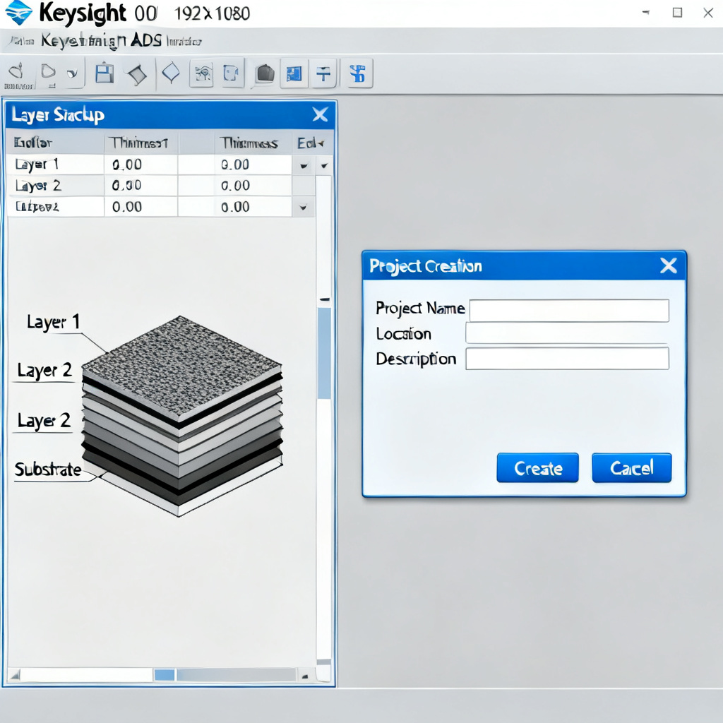
Create a New Project and Define the Layer Stackup
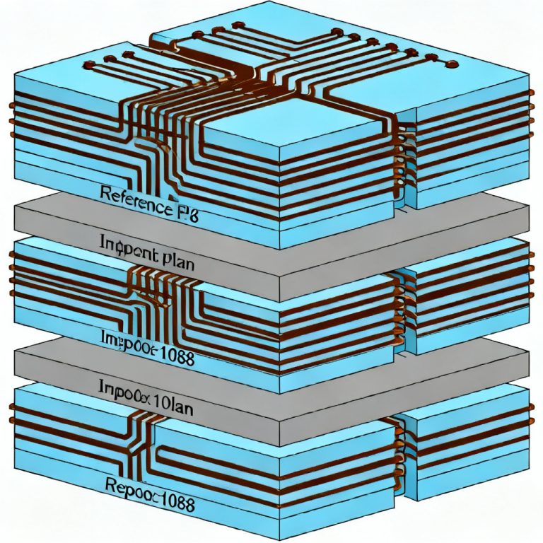
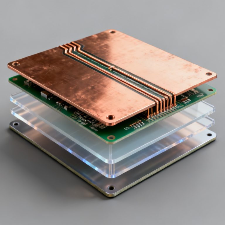
Launch ADS and navigate to File > New > Project. Name it, e.g., “Crosstalk_Analysis_PCB.” Set the Technology to a standard PCB stackup (e.g., FR4 with Dk=4.5, loss tangent=0.02) or import your custom layer stack from your PCB design tool. Go to Momentum > Substrate Editor or Layout > Stackup. Specify the number of layers (e.g., 4-layer: top signal, GND, power, bottom signal). Enter dielectric thickness (e.g., 0.2 mm for prepreg), copper thickness (1 oz = 0.035 mm), and material properties.
Pro Tip from Cadence: Always include a solid reference plane (GND) to reduce common-mode crosstalk.
Import or Draw the PCB Layout
Option A: Import from Allegro/Altium: Use File > Import > DXF/ODB++ to bring in your existing layout. This ensures real-world geometry.
Option B: Draw Test Structures: For learning, draw two parallel microstrip lines using the Layout > Line tool. Set length = 100 mm, width = 0.2 mm, spacing = 0.2 mm (S/H = 1).
Step 3: Configuring the Crosstalk Simulation in Keysight ADS
This is the core of the crosstalk analysis in high speed PCB. The three authoritative sources converge on the following workflow.
Choose the Simulation Type and Set Up Ports
For Single-Ended Traces: Use S-Parameter Simulation with a Momentum RF or FEM solver. This provides frequency-domain crosstalk (S31 for NEXT, S41 for FEXT).
For Differential Pairs: Use Differential S-Parameters (SDD21, SDD31). Keysight’s documentation recommends using the Circuit Envelope or Transient simulator for time-domain analysis.
Assign Port 1 to the aggressor’s input, Port 2 to the aggressor’s output, Port 3 to the victim’s near end, and Port 4 to the victim’s far end. Set port impedance to 50 ohms (common for high-speed designs).
Best Practice from Altium: Use internal ports with a S-parameter block to model the trace as a distributed transmission line.
Define the Simulation Frequency Range and Run
For high-speed designs, sweep from DC to 5x the fundamental frequency (e.g., for 10 Gbps, sweep to 50 GHz). Use adaptive frequency sampling (e.g., 100 points per decade) to capture resonance peaks. Click Simulate in the Momentum toolbar. For large layouts, use FEM for higher accuracy. Expect simulation time of 1-5 minutes for simple structures.
Step 4: Analyzing the Crosstalk Results in High Speed PCB
After simulation, ADS provides multiple ways to visualize crosstalk in high speed PCB. Here’s how to interpret them.
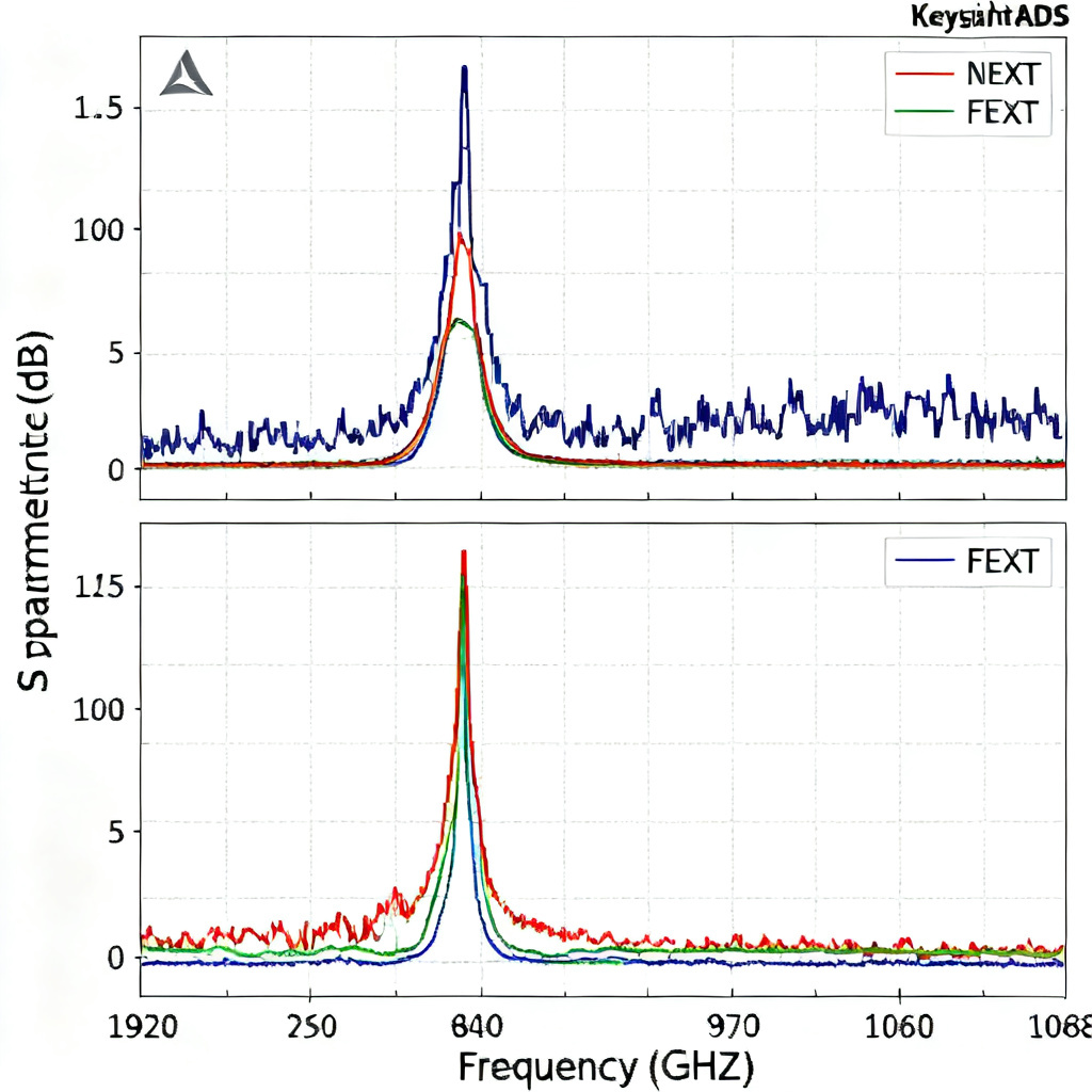
Frequency-Domain Analysis with S-Parameters
Plot S31 (NEXT): This shows the coupling from aggressor input to victim near end. A typical value for S/H=1 is around -20 dB at 1 GHz. If S31 exceeds -15 dB, crosstalk is problematic.
Plot S41 (FEXT): This is often lower than NEXT. For microstrip, FEXT can be positive due to inductive coupling; for stripline, it is near zero.
Source Insight: Keysight’s documentation emphasizes that S-parameter plots reveal the frequency-dependent nature of crosstalk. A peak at a specific frequency indicates a resonance due to stub or via effects.
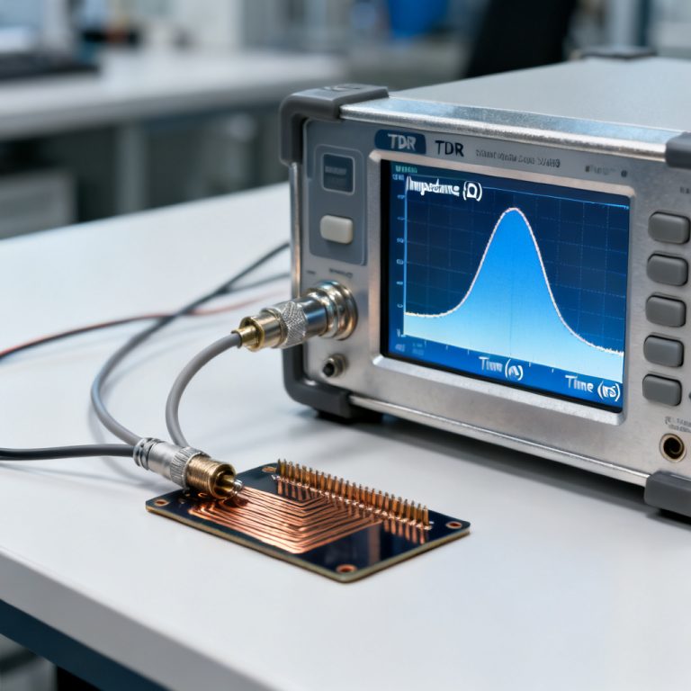
Time-Domain Analysis with TDR/TDT
Use Transient Simulation with a step source (e.g., 0 to 1V with 50 ps rise time). Plot Vout at Port 3 (NEXT): You will see a positive pulse with amplitude proportional to coupling length. Plot Vout at Port 4 (FEXT): For microstrip, the pulse shape follows the derivative of the aggressor signal.
Cadence Approach: Compare the victim’s noise margin (e.g., 150 mV for LVDS) against the crosstalk amplitude. If crosstalk > 10% of the signal swing, redesign is needed.
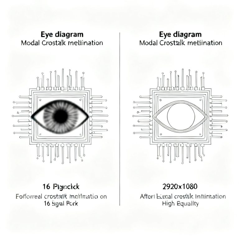
Eye Diagram Analysis for High-Speed Digital
For high-speed digital, use the Eye Diagram tool in ADS. Inject a PRBS pattern (e.g., PRBS7) into the aggressor and observe the victim’s eye closure. Key Metric: Eye height and width degradation. A 10% reduction in eye height due to crosstalk is the typical limit.
Step 5: Mitigating Crosstalk in Your High Speed PCB Design
Based on the simulation results, you can implement these proven techniques for crosstalk reduction in high speed PCB.
Increase Trace Spacing and Use Guard Traces
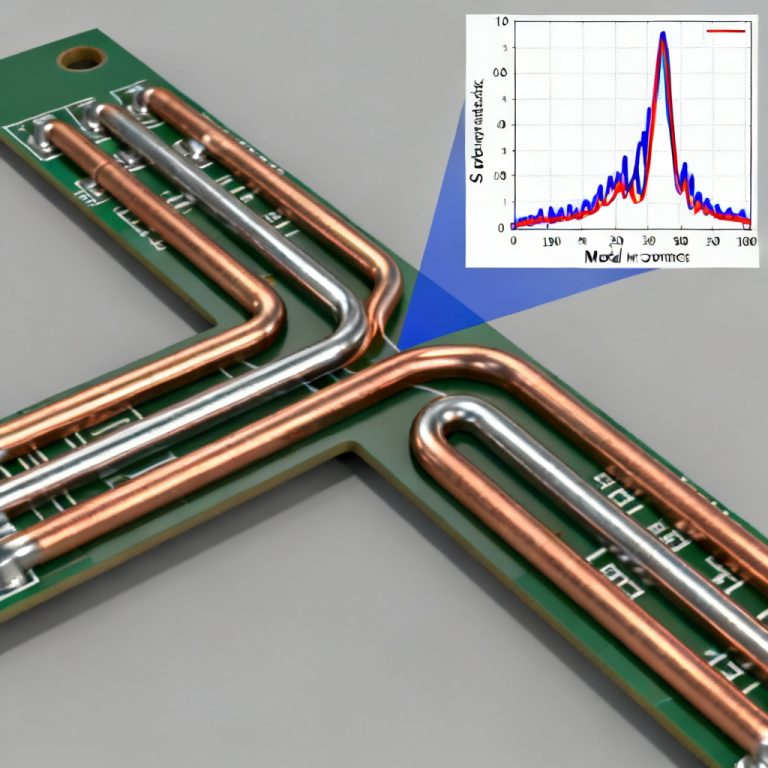
This is the most effective method. From your ADS simulation, plot crosstalk vs. spacing. The rule of thumb: S ≥ 3H (e.g., for H=0.2 mm, S ≥ 0.6 mm). For high-speed signals (≥ 5 Gbps), use S ≥ 5H. Altium’s Recommendation: Use a 3W rule (trace width = W, spacing = 3W) for critical nets.
Place a grounded trace between aggressor and victim. In ADS, add a third trace and connect it to GND via vias. Simulation Insight: A guard trace with vias spaced at λ/10 (e.g., every 3 mm at 10 GHz) can reduce crosstalk by 10-15 dB. Without vias, it may worsen crosstalk due to parasitic coupling.
Optimize Layer Stackup and Minimize Parallel Run Length
Use stripline (inner layers) instead of microstrip. In ADS, move the traces to an inner layer between two GND planes. FEXT is nearly eliminated in stripline. Reduce dielectric height (H) to lower the coupling field. For example, H=0.1 mm reduces crosstalk by 6 dB compared to H=0.2 mm.
For critical differential pairs, limit parallel run length to < 1 inch. Use ADS to simulate the effect of length on FEXT amplitude.
Termination, Impedance Matching, and Differential Pair Routing
Add series or parallel termination to reduce reflections that amplify crosstalk. In ADS, use a Term component with 50 ohms. Route high-speed signals as differential pairs. In ADS, simulate SDD21 vs. SCC21 (common-mode crosstalk). Differential pairs offer 20-30 dB better crosstalk immunity than single-ended.
Step 6: Advanced Techniques with Keysight ADS for High Speed PCB Crosstalk
For B2B engineers handling complex designs, ADS offers advanced features for crosstalk analysis in high speed PCB.
Electromagnetic Co-Simulation and Statistical Eye Analysis
Use ADS Momentum to perform full-wave EM simulation of the entire board region. This captures via coupling, plane resonances, and return path discontinuities. Workflow: Export the layout, define the EM model, and co-simulate with circuit elements (e.g., drivers, receivers).
Use the Channel Simulator in ADS to run Monte Carlo analysis with process variations (e.g., ±10% in Dk, ±20% in trace width). This predicts yield for your PCB.
Crosstalk De-embedding for Measurement Correlation
For measurement correlation, use ADS’s De-embedding tool to remove fixture effects. This is critical for validating your simulation against real-world prototypes.
Step 7: Validating Your High Speed PCB Design with Prototyping
Simulation is only half the battle. For B2B PCB manufacturing, you must validate with physical prototypes to confirm crosstalk in high speed PCB.
Fabricate Test Coupons and Measure with VNA
Include a crosstalk test structure (e.g., two 100 mm traces with variable spacing) on your PCB panel. This allows TDR measurements. Use a Vector Network Analyzer (VNA) to measure S-parameters up to 50 GHz. Compare with ADS results; a mismatch of < 2 dB is acceptable.
For time-domain, use a sampling oscilloscope with TDR module. The crosstalk pulse shape should match ADS transient simulation. If measured crosstalk exceeds -20 dB, return to ADS to adjust spacing, stackup, or guard traces. This iterative process ensures first-pass success.
Conclusion: Leveraging Keysight ADS for High Speed PCB Success
Crosstalk analysis in high speed PCB with Keysight ADS is not just a simulation—it’s a strategic tool for B2B PCB manufacturers and designers. By following this step-by-step guide, you can:
- Identify crosstalk issues early in the design phase.
- Optimize layout parameters (spacing, stackup, guard traces) for minimal coupling.
- Validate designs with EM co-simulation and statistical analysis.
- Reduce prototyping costs and time-to-market.
For your next high-speed PCB project (e.g., 10 Gbps SerDes, DDR5, or RF front-ends), integrate ADS crosstalk analysis into your workflow. The combination of physics-based simulation and proven mitigation techniques ensures robust, reliable, and manufacturable designs.
Need help fabricating your high-speed PCB? Contact us for a free DFM review. Our advanced manufacturing capabilities support complex stackups, tight impedance tolerances, and high-density interconnects—backed by simulation-driven design.
Frequently Asked Questions about Crosstalk Analysis in High Speed PCB with Keysight ADS
What is crosstalk analysis in high speed PCB?
Crosstalk analysis in high speed PCB is the process of evaluating unwanted electromagnetic coupling between adjacent traces, which can degrade signal integrity. Keysight ADS provides a physics-based simulation environment to model and mitigate this coupling.
How do I perform crosstalk analysis in high speed PCB with Keysight ADS?
To perform crosstalk analysis in high speed PCB with Keysight ADS, set up a project with the correct layer stackup, import or draw the PCB layout, configure S-parameter or transient simulations, and analyze NEXT and FEXT results to guide design improvements.
What are the best practices for crosstalk reduction in high speed PCB?
Best practices for crosstalk reduction in high speed PCB include increasing trace spacing (S ≥ 3H), using guard traces with vias, optimizing layer stackup with stripline, minimizing parallel run length, and employing differential pair routing.
Why is Keysight ADS recommended for crosstalk analysis in high speed PCB?
Keysight ADS is recommended for crosstalk analysis in high speed PCB because it offers full-wave EM simulation, statistical eye analysis, and de-embedding tools, enabling accurate prediction and validation of crosstalk effects in complex designs.
What is the difference between NEXT and FEXT in crosstalk analysis in high speed PCB?
In crosstalk analysis in high speed PCB, NEXT (Near-End Crosstalk) is measured at the aggressor’s driving end and is influenced by mutual capacitance and inductance, while FEXT (Far-End Crosstalk) is measured at the victim’s far end and is more sensitive to propagation delay differences.
| Parameter | Description for Crosstalk Analysis in High Speed PCB |
|---|---|
| Trace Spacing (S) | Distance between adjacent traces; S ≥ 3H is a common rule for crosstalk reduction. |
| Dielectric Height (H) | Thickness of dielectric material; reducing H lowers coupling field. |
| Guard Traces | Grounded trace between aggressor and victim; vias spaced at λ/10 enhance effectiveness. |
| Stripline vs Microstrip | Stripline offers lower FEXT due to homogeneous medium; microstrip has higher FEXT. |
| Differential Pair Routing | Provides 20-30 dB better crosstalk immunity compared to single-ended traces. |
Comparison: Keysight ADS vs Other Tools for Crosstalk Analysis in High Speed PCB
When evaluating tools for crosstalk analysis in high speed PCB, Keysight ADS stands out for its full-wave EM capabilities and integration with measurement equipment. Altium Designer offers a more accessible interface for layout engineers, while Cadence Sigrity provides robust statistical analysis. However, ADS excels in high-frequency accuracy and de-embedding for validation.
Glossary of Key Terms for Crosstalk Analysis in High Speed PCB
Capacitive Coupling: Electric field interaction between traces contributing to crosstalk.
Inductive Coupling: Magnetic field interaction between traces contributing to crosstalk.
Near-End Crosstalk (NEXT): Crosstalk measured at the aggressor’s driving end.
Far-End Crosstalk (FEXT): Crosstalk measured at the victim’s far end.
Guard Trace: A grounded trace placed between aggressor and victim to reduce coupling.
Stripline: A transmission line embedded between two reference planes, offering lower crosstalk.
Microstrip: A transmission line on an outer layer, more susceptible to crosstalk.
3W Rule: A design guideline where trace spacing is three times the trace width.