[rank_math_breadcrumb]
Master differential pair impedance verification with VNA and mixed-mode S-parameters. Learn TDR vs. VNA, calibration, de-embedding, and design optimization for high-speed PCBs.
Introduction to Differential Pair Impedance Verification Using VNA
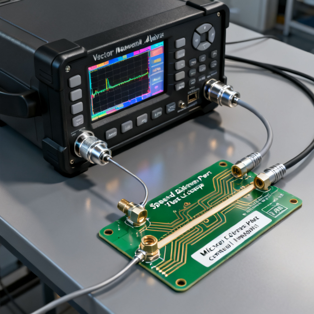
Differential pair impedance verification using VNA is essential for high-speed digital design. From PCIe Gen 5 to USB4 and 100GbE, differential signaling relies on precise impedance control to maintain signal quality and minimize electromagnetic interference. While Time Domain Reflectometry (TDR) has long been the go-to method for impedance verification, Vector Network Analyzers (VNAs) combined with mixed-mode S-parameters offer a superior, frequency-domain alternative. This pillar page provides an exhaustive guide to differential pair impedance verification using VNA and mixed-mode S-parameters, synthesizing best practices from leading industry sources.
Why VNA for Differential Pair Impedance Verification?
Differential pair impedance verification using VNA overcomes TDR limitations. Traditional TDR measurements provide a time-domain snapshot of impedance along a transmission line. However, for modern high-speed designs operating at multi-gigahertz frequencies, TDR has limitations:
- Bandwidth Constraints: TDR risetime limits the resolution of small impedance discontinuities.
- Frequency-Dependent Losses: TDR cannot directly characterize dielectric and conductor losses that vary with frequency.
- Limited to Single-Ended or Simple Differential: TDR struggles with complex mixed-mode measurements without post-processing.
VNAs overcome these challenges by measuring in the frequency domain, offering:
- Wider Bandwidth: VNAs can measure up to 110 GHz and beyond, capturing impedance variations at high frequencies.
- Comprehensive Characterization: S-parameters provide full reflection and transmission data, enabling extraction of differential impedance (Zdiff), common-mode impedance (Zcm), and mode conversion (Scd21, Sdc21).
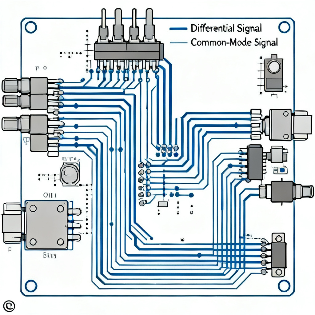
- Mixed-Mode S-Parameters: This is the cornerstone. Mixed-mode S-parameters (Sdd, Scc, Scd, Sdc) transform standard single-ended 4-port S-parameters into differential and common-mode components, directly revealing impedance mismatches and asymmetry.
Understanding Mixed-Mode S-Parameters for Impedance Verification
Differential pair impedance verification using VNA relies on mixed-mode S-parameters. Mixed-mode S-parameters are a mathematical transformation of standard 4-port S-parameters (for a differential pair). They are defined as:
- Sdd (Differential Mode): Differential reflection (Sdd11) and differential transmission (Sdd21). This directly indicates the differential impedance match and insertion loss.
- Scc (Common Mode): Common-mode reflection (Scc11) and common-mode transmission (Scc21). High common-mode reflection indicates poor common-mode impedance control.
- Scd (Mode Conversion: Common to Differential): Measures how much common-mode energy is converted to differential mode—a critical metric for EMI and signal integrity.
- Sdc (Mode Conversion: Differential to Common): Measures how much differential energy is converted to common mode—a key indicator of asymmetry or skew.
Verification of differential pair impedance is achieved by analyzing Sdd11 (return loss) and converting it to impedance using the formula:
Zdiff = Z0 × (1 + Sdd11) / (1 – Sdd11)
Where Z0 is the reference impedance (typically 100 Ω for differential pairs).
Key Mixed-Mode S-Parameter Terms Explained
Differential pair impedance verification using VNA requires understanding these terms: Sdd11 is differential return loss; Sdd21 is differential insertion loss; Scd21 and Sdc21 quantify mode conversion. Mode conversion above -30 dB indicates asymmetry.
Step-by-Step VNA Measurement Process for Differential Pairs
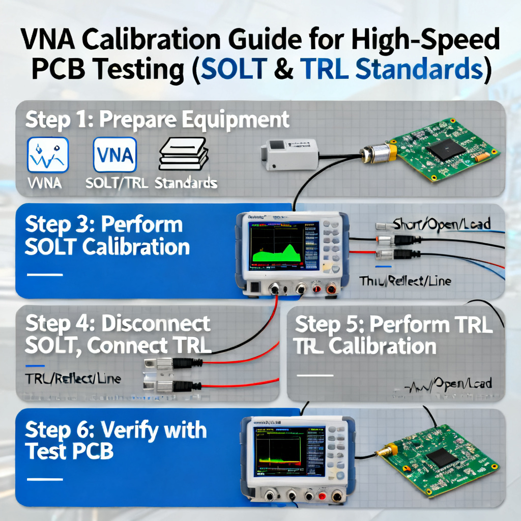
Differential pair impedance verification using VNA follows a rigorous procedure. To obtain accurate mixed-mode S-parameters, follow this rigorous procedure:
1. Calibration: The Foundation of Accuracy
- SOLT (Short-Open-Load-Thru) Calibration: Use a precision calibration kit (e.g., 85052D) at the VNA ports. For differential measurements, a 4-port SOLT calibration is essential.
- TRL (Thru-Reflect-Line) Calibration: Preferred for on-wafer or board-level measurements due to its independence from known standards. Requires a set of calibration standards on the same substrate as the DUT.
- Important: Calibrate to the reference plane where the DUT begins (e.g., at the SMA connector launch). This removes the effects of cables and adapters.
2. Fixturing and Cabling
- Use phase-matched, low-loss coaxial cables (e.g., Gore or Times Microwave) to minimize phase and amplitude imbalance.
- For differential probes (e.g., GGB Industries or Cascade Microtech), ensure the probe pitch matches the DUT pad geometry.
- Avoid: Long, unmatched cables that introduce skew and loss.
3. De-embedding: Removing Fixture Effects
When the DUT is embedded in a test fixture (common for PCB coupons), de-embedding is critical. Methods include:
- 2x-Thru Method: Measure a thru line of identical length and subtract its S-parameters using algorithms (e.g., in Keysight PLTS or ADS).
- L-2L Method: Use two lines of different lengths to extract fixture parasitics.
- TRL De-embedding: Use the same TRL standards from calibration but applied to the fixture.
4. Data Acquisition and Post-Processing
- Set frequency sweep from low (e.g., 10 MHz) to the maximum frequency of interest (e.g., 40 GHz for 28 Gbps signals).
- Use intermediate frequency bandwidth (IFBW) of 1 kHz to 10 kHz for low noise.
- Export S-parameter Touchstone files (.s4p for 4-port data).
5. Mixed-Mode Transformation
- Use VNA software (e.g., Keysight PLTS, Anritsu ShockLine, or open-source tools) to convert single-ended S-parameters to mixed-mode.
- Examine Sdd11 (differential return loss). A return loss < -15 dB at the operating frequency indicates good impedance matching.
- Compute Zdiff from Sdd11. A deviation of ±10% from 100 Ω is typical for high-speed designs; ±5% is excellent.
Interpreting Mixed-Mode S-Parameters for Impedance Verification
Differential pair impedance verification using VNA requires data interpretation. Here are case studies:
| Case | Sdd11 | Scc11 | Scd21 / Sdc21 | Zdiff | Interpretation |
|---|---|---|---|---|---|
| Balanced Pair (Ideal) | < -20 dB | < -20 dB | < -30 dB | 100 Ω ± 2% | Excellent impedance control |
| Asymmetric Pair | -10 to -15 dB | Low | -20 to -30 dB | Varies with frequency | Skew or width mismatch |
| Common-Mode Mismatch | Good | > -10 dB | Elevated | May be nominal | Poor common-mode termination |
| Via/Connector Discontinuity | Sharp dips/peaks | Variable | Variable | Spikes (e.g., 120 Ω) | Resonance at via transitions |
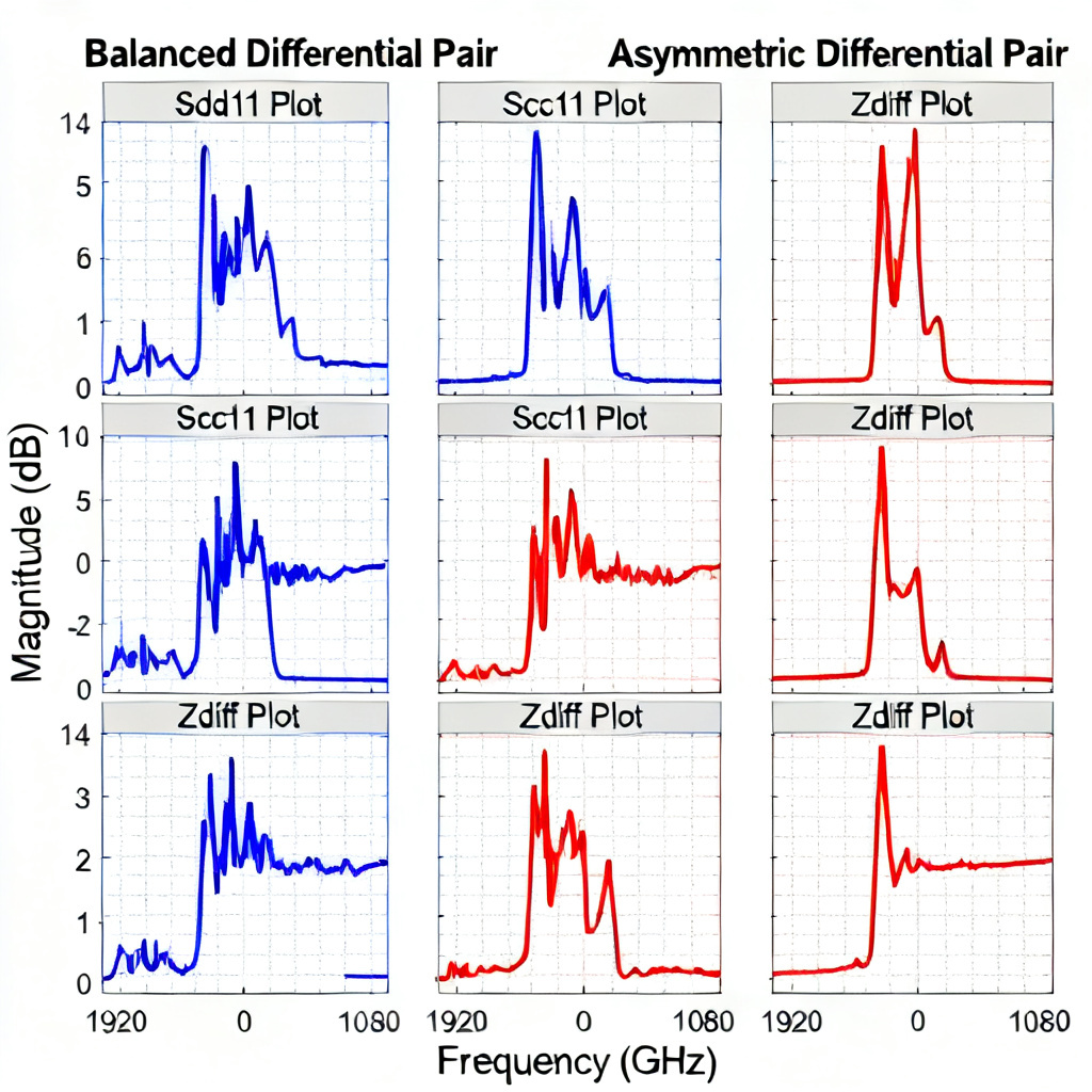
Case 1: Balanced Differential Pair (Ideal)
- Sdd11: Low (< -20 dB) across the band.
- Scc11: Low (< -20 dB).
- Scd21 and Sdc21: Very low (< -30 dB). No mode conversion.
- Zdiff: 100 Ω ± 2%.
Case 2: Asymmetric Pair (e.g., Skew or Width Mismatch)
- Sdd11: Moderate (-10 to -15 dB) with ripples.
- Scc11: May be low, but Scd21 and Sdc21 are elevated (e.g., -20 to -30 dB).
- Zdiff: Varies with frequency; impedance may be high or low at specific harmonics.
- Action: Inspect physical layout for length mismatch, dielectric thickness variation, or etch tolerance.
Case 3: Common-Mode Impedance Mismatch
- Scc11: High (> -10 dB).
- Sdd11: May still be good, but Scc11 indicates poor common-mode termination.
- Action: Check common-mode impedance of the differential pair (target: 25-50 Ω, depending on design). Adjust trace geometry or add common-mode filters.
Case 4: Via or Connector Discontinuities
- Sdd11: Sharp dips or peaks at specific frequencies (resonances).
- Zdiff: Localized impedance spikes (e.g., 120 Ω) at via transitions.
- Action: Optimize via anti-pad, back-drilling, or use ground stitching vias.
Comparison with TDR for Impedance Verification
Differential pair impedance verification using VNA vs. TDR:
| Feature | TDR | VNA with Mixed-Mode S-Parameters |
|---|---|---|
| Measurement Domain | Time | Frequency |
| Frequency Range | Limited by risetime | Full bandwidth (DC to >100 GHz) |
| Impedance Resolution | Good for discontinuities | Excellent for lossy, dispersive lines |
| Loss Characterization | Indirect (through impedance ripple) | Direct (Sdd21 magnitude and phase) |
| Mode Conversion | Requires post-processing | Directly provided (Scd21, Sdc21) |
| Calibration Complexity | Simple (open/short) | Complex (SOLT/TRL) |
| Cost | Lower | Higher |
Best Practices for High-Speed PCB Design Verification
- Use VNA for Final Verification: While TDR is useful for quick checks, VNA mixed-mode S-parameters provide the most accurate impedance and loss data for high-speed designs.
- Include Test Coupons: Design dedicated test coupons with the same stackup and trace geometry as the differential pair. Include multiple lengths for de-embedding.
- Correlate with Simulation: Compare measured mixed-mode S-parameters with 3D EM simulations (e.g., Ansys HFSS, CST) to validate models.
- Monitor Mode Conversion: Scd21 and Sdc21 should be < -30 dB for robust designs. Higher values indicate asymmetry that can cause EMI and jitter.
- Consider Temperature and Process Variation: Measure multiple samples across temperature (-40°C to 125°C) to ensure robust performance.
Common Pitfalls and How to Avoid Them
- Inadequate Calibration: Using a 2-port calibration for a 4-port measurement leads to errors. Always perform full 4-port SOLT or TRL.
- Ignoring Cable Phase Imbalance: Even with phase-matched cables, test for imbalance by measuring a short thru. If Scd21 > -40 dB, replace cables.
- Neglecting De-embedding: Measuring through a long fixture without de-embedding yields inaccurate Zdiff. Always de-embed to the DUT reference plane.
- Misinterpreting Sdd11: A low Sdd11 does not guarantee good impedance—it only indicates that the impedance is close to the reference. Always convert to Zdiff for verification.
FAQ: Differential Pair Impedance Verification Using VNA
What is differential pair impedance verification using VNA?
Differential pair impedance verification using VNA is a frequency-domain method that uses mixed-mode S-parameters to measure and validate the differential impedance of high-speed PCB interconnects.
How does mixed-mode S-parameter analysis improve differential pair impedance verification?
Mixed-mode S-parameters provide direct measurements of differential and common-mode behavior, including mode conversion, which is critical for accurate differential pair impedance verification.
What is the difference between TDR and VNA for differential pair impedance verification?
TDR measures impedance in the time domain with limited bandwidth, while VNA with mixed-mode S-parameters offers full frequency characterization, loss analysis, and mode conversion data for precise differential pair impedance verification.
Why is calibration important for differential pair impedance verification using VNA?
Calibration removes systematic errors from cables and adapters, ensuring that the measured S-parameters accurately represent the DUT for reliable differential pair impedance verification.
What does mode conversion (Scd21, Sdc21) indicate in differential pair impedance verification?
Mode conversion indicates asymmetry in the differential pair; high values suggest poor impedance balance, which can degrade signal integrity and require design adjustments.
Conclusion
Differential pair impedance verification using VNA and mixed-mode S-parameters is the gold standard for high-speed PCB design. By mastering calibration, de-embedding, and mixed-mode transformation, engineers can achieve precise impedance control, minimize mode conversion, and ensure signal integrity up to 100+ GHz. This approach not only validates design intent but also provides actionable data for manufacturing optimization.
For custom high-speed PCB fabrication and assembly, our facility utilizes VNA-based verification to guarantee differential impedance within ±5% of target, ensuring your designs meet the most stringent performance requirements. Contact us for a free design review and impedance test coupon analysis.