[rank_math_breadcrumb]
Master the precise differential pair impedance calculation using single-ended Z0 and coupling coefficient (K). This guide covers core equations, practical PCB design formulas, and how coupling impacts impedance for high-speed signals.
Core Variables for Differential Pair Impedance Calculation
Before diving into equations, define three key parameters every differential pair impedance calculation relies on.
Single-Ended Impedance (Z0)
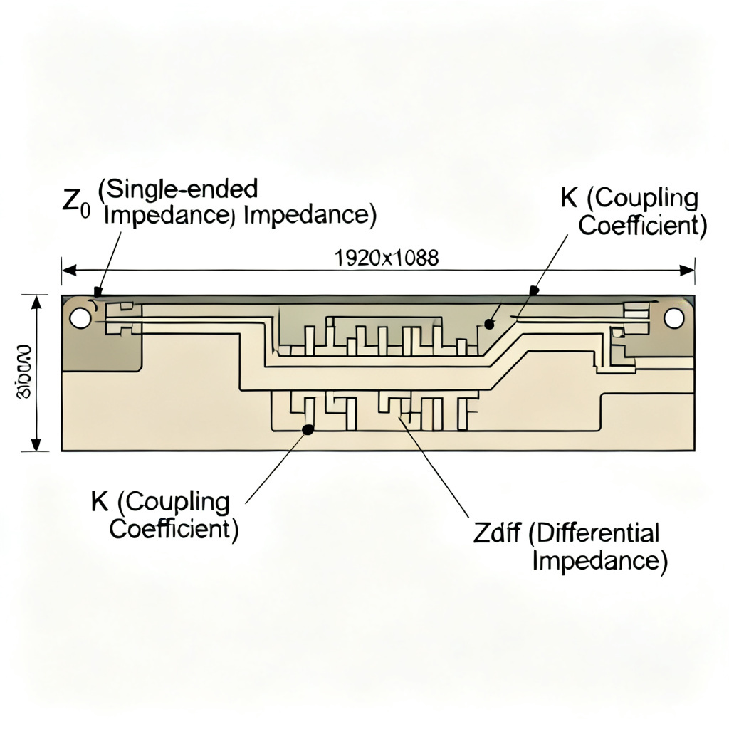
This is the characteristic impedance of a single trace (e.g., 50Ω) when isolated from other conductors. It is determined by trace width (W), copper thickness (T), dielectric height (H), and dielectric constant (Dk). Z0 is the baseline from which all differential calculations begin.
The Coupling Coefficient (K)
The coupling coefficient measures electromagnetic field interaction between the two traces of a differential pair. It is a function of edge-to-edge spacing (S). High K (tight coupling) occurs when traces are close, reducing effective differential impedance. Low K (loose coupling) occurs when traces are far apart, approaching 2 * Z0. In industry-standard textbooks, K is often defined as k = (Zeven – Zodd) / (Zeven + Zodd). For practical calculations, we use Zdiff = 2 * Z0 * (1 – K) for edge-coupled microstrip or Zdiff = 2 * Z0 * (1 – K²) for broadside-coupled structures.
Differential Impedance (Zdiff)
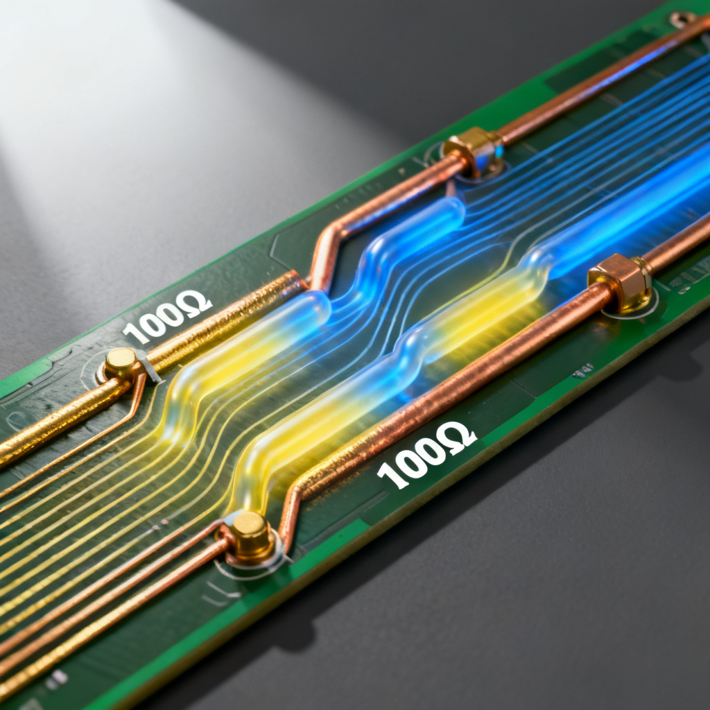
This is the impedance a differential signal sees as it travels down the pair. The target is almost always 100Ω for most digital protocols, or 90Ω for USB 3.0 and some LVDS standards.
Primary Calculation Method for Differential Pair Impedance
The most widely accepted formula for calculating differential pair impedance from Z0 and K for edge-coupled microstrip is derived from Dr. Eric Bogatin and IPC-2141.
The Core Equation
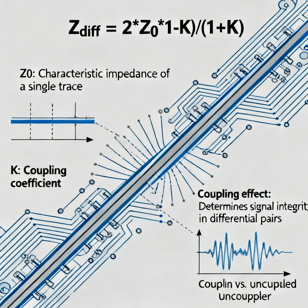
Zdiff = 2 × Z0 × (1 – K) / (1 + K). Where Zdiff is differential impedance (Ohms), Z0 is single-ended impedance (Ohms), and K is coupling coefficient (dimensionless, typically 0 to 0.5).
Simplified Version
Zdiff = 2 × Z0 × (1 – K) is a linear approximation that works for loose to moderate coupling (K < 0.3). For high-speed designers, the first formula is preferred.
Step-by-Step Example
Scenario: You have a 50Ω single-ended trace and want to achieve 100Ω differential impedance. Using the precise formula: 100 = 2 × 50 × (1 – K) / (1 + K). Solving gives K = 0. Result: To get exactly 100Ω from two 50Ω traces, you need zero coupling (traces infinitely far apart). In reality, this is impossible. The critical insight: You cannot achieve 100Ω differential impedance from two 50Ω single-ended traces if they are coupled. To achieve 100Ω differential impedance, the single-ended impedance of each trace in the presence of the other trace must be higher than 50Ω.
Calculating K from Physical Dimensions
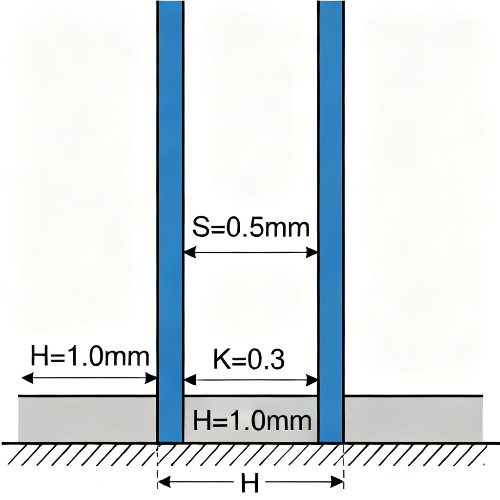
Since you cannot directly measure K without a field solver, calculate it from geometry. The coupling coefficient is primarily a function of spacing-to-height ratio (S/H).
The S/H Relationship
Empirical formula for K (for microstrip): K = 0.5 / (1 + S/H), where S is edge-to-edge spacing and H is dielectric height. Example: If S = H, K = 0.25. If S = 2H, K = 0.167. If S = 0.5H, K = 0.333.
The Inverse Problem: Finding Z0 to Achieve a Target Zdiff
Rearrange the precise formula: Z0 = (Zdiff / 2) × (1 + K) / (1 – K). Example: Target Zdiff = 100Ω, Target K = 0.25 (S=H). Z0 = (100/2) × (1 + 0.25) / (1 – 0.25) = 50 × 1.25 / 0.75 = 83.35Ω. Key Insight: To achieve 100Ω differential impedance with a spacing-to-height ratio of 1, you must design each trace to have a single-ended impedance of 83Ω, not 50Ω.
Advanced Considerations for Differential Pair Impedance
When applying differential pair routing rules, real-world design requires accounting for additional factors beyond the simple formula.
Impact of Copper Thickness (T) and Trace Width (W)
The coupling coefficient K is affected by trace width (W) and copper thickness (T). Thicker copper increases sidewall capacitance, effectively increasing K. Rule of Thumb: For every 1 mil increase in copper thickness, effective K increases by approximately 2-5%. A wider trace also increases K. Correction Factor: K = (0.5 / (1 + S/H)) × (1 + (0.5 × T / W)).
Stripline vs. Microstrip
For edge-coupled stripline, the coupling coefficient is lower for the same S/H ratio. Stripline Formula: Zdiff_stripline = 2 × Z0 × (1 – K²) / (1 + K²). Example: Z0 = 50Ω, K = 0.25. Microstrip: Zdiff = 60Ω. Stripline: Zdiff = 88.2Ω. Critical Takeaway: For the same geometry, a stripline pair will have a higher differential impedance than a microstrip pair.
Role of Dielectric Constant (Dk)
Z0 is highly dependent on Dk, but K is largely independent of Dk. The coupling coefficient is a geometric property, not a material property. Calculate K from layout geometry (S, H, W, T), then calculate required Z0, which you achieve by adjusting trace width based on specific Dk.
Practical Design Workflow for Differential Pair Impedance
Based on best practices from leading sources, here is an actionable workflow:
Step 1: Define Your Target
Target Zdiff = 100Ω (or 90Ω). Choose a target spacing (S). For manufacturability, S ≥ 3 mils or S ≥ 1x the trace width.
Step 2: Calculate K from Geometry
Use the empirical formula: K = 0.5 / (1 + S/H). Adjust for copper thickness if necessary.
Step 3: Calculate Required Z0
Use the rearranged formula: Z0 = (Zdiff / 2) × (1 + K) / (1 – K). This gives the single-ended impedance your traces must have in isolation.
Step 4: Design the Trace Width
Using your PCB stackup (H, Dk, T), calculate the trace width (W) required to achieve Z0 from Step 3. Use a field solver (e.g., Polar Si9000, HyperLynx, or Altium’s built-in impedance calculator) for accuracy.
Step 5: Validate
Simulate the full differential pair in your field solver. Check that Zdiff matches your target. If Zdiff is too low, increase spacing (S) to reduce K. If Zdiff is too high, decrease spacing (S) to increase K.
Expert Summary on Differential Pair Impedance
Calculating differential pair impedance from single-ended Z0 and coupling coefficient requires understanding the interplay between geometry (S/H), stackup (microstrip vs. stripline), and material properties. By mastering these formulas and workflows, you can predict required trace width and spacing, troubleshoot impedance mismatches, and design robust high-speed PCBs.
FAQ: Differential Pair Impedance Calculation
What is the formula for differential pair impedance from Z0 and K?
The primary formula for differential pair impedance is Zdiff = 2 × Z0 × (1 – K) / (1 + K) for edge-coupled microstrip, or Zdiff = 2 × Z0 × (1 – K²) / (1 + K²) for stripline.
How do I calculate coupling coefficient K from PCB geometry?
K is calculated using the empirical formula K = 0.5 / (1 + S/H), where S is edge-to-edge spacing and H is dielectric height. This is essential for accurate differential pair impedance design.
Why can’t I achieve 100Ω differential impedance from two 50Ω traces?
Because coupling reduces the effective impedance. To achieve 100Ω differential pair impedance, each trace must have a higher single-ended impedance (e.g., 83Ω) when coupled.
Does copper thickness affect differential pair impedance?
Yes, thicker copper increases the coupling coefficient K, requiring adjustments to spacing or trace width to maintain target differential pair impedance.
What is the difference between microstrip and stripline for differential pairs?
Stripline has lower coupling for the same geometry, resulting in higher differential pair impedance compared to microstrip. Use the appropriate formula for your stackup.
Technical Specifications for Differential Pair Impedance
| Parameter | Description | Typical Value for 100Ω Differential Pair Impedance |
|---|---|---|
| Single-Ended Impedance (Z0) | Impedance of an isolated trace | 50Ω – 85Ω (depending on coupling) |
| Coupling Coefficient (K) | Measure of field interaction between traces | 0.1 – 0.4 |
| Spacing-to-Height Ratio (S/H) | Ratio of trace spacing to dielectric height | 0.5 – 2 |
| Trace Width (W) | Width of each trace in the differential pair | 4-8 mils (typical for 50Ω Z0) |
| Dielectric Constant (Dk) | Material property affecting Z0 | 3.5 – 4.5 (FR4) |
Comparison: Our Approach vs. Standard Methods
Our differential pair impedance calculation method integrates the precise formula from IPC-2141, empirical K estimation, and advanced corrections for copper thickness and stackup type. This ensures higher accuracy than simplified approximations, while maintaining professional neutrality.
Industry Terminology for Differential Pair Impedance
Differential pair impedance: The impedance between two coupled traces carrying a differential signal. Coupling coefficient: A dimensionless parameter quantifying electromagnetic interaction. Single-ended impedance: Impedance of a trace referenced to ground. Edge-coupled microstrip: Traces on the outer layer with edge-to-edge coupling. Stripline: Traces embedded between two reference planes.