Eye Diagram PCB analysis in Keysight ADS is the definitive method for validating signal integrity in high-speed digital designs. This practical guide equips you to master eye diagram measurements, interpret key metrics, and apply advanced ADS simulation techniques to ensure your high-speed PCB meets rigorous performance standards.
- 1. Understanding the Eye Diagram – Theory and Key Metrics for Eye Diagram PCB Analysis
- 2. Setting Up Eye Diagram Analysis in Keysight ADS for Your PCB
- 3. Advanced Analysis and Interpretation in Keysight ADS for Eye Diagram PCB Analysis
- 4. Practical Troubleshooting – Common Issues in Eye Diagram PCB Analysis
- 5. Best Practices for High-Speed PCB Design Using ADS Eye Analysis
- FAQ
1. Understanding the Eye Diagram – Theory and Key Metrics for Eye Diagram PCB Analysis
Eye Diagram PCB analysis begins with a solid grasp of what an eye diagram represents and what it reveals about signal quality. An eye diagram is created by overlaying multiple segments of a digital signal, triggered by a clock or data pattern, forming an image that resembles a human eye. The openness of the eye directly correlates to signal quality: a wide, clear eye indicates low noise and jitter, while a closed, distorted eye signals potential communication errors.
1.1 What Is an Eye Diagram in High-Speed PCB Design?
In high-speed PCB design, the eye diagram provides a statistical view of a signal’s behavior over many transitions. It reveals noise, timing errors, and amplitude distortions at a glance, making it the most powerful and intuitive tool for signal integrity analysis.
1.2 Key Metrics Measured from an Eye Diagram
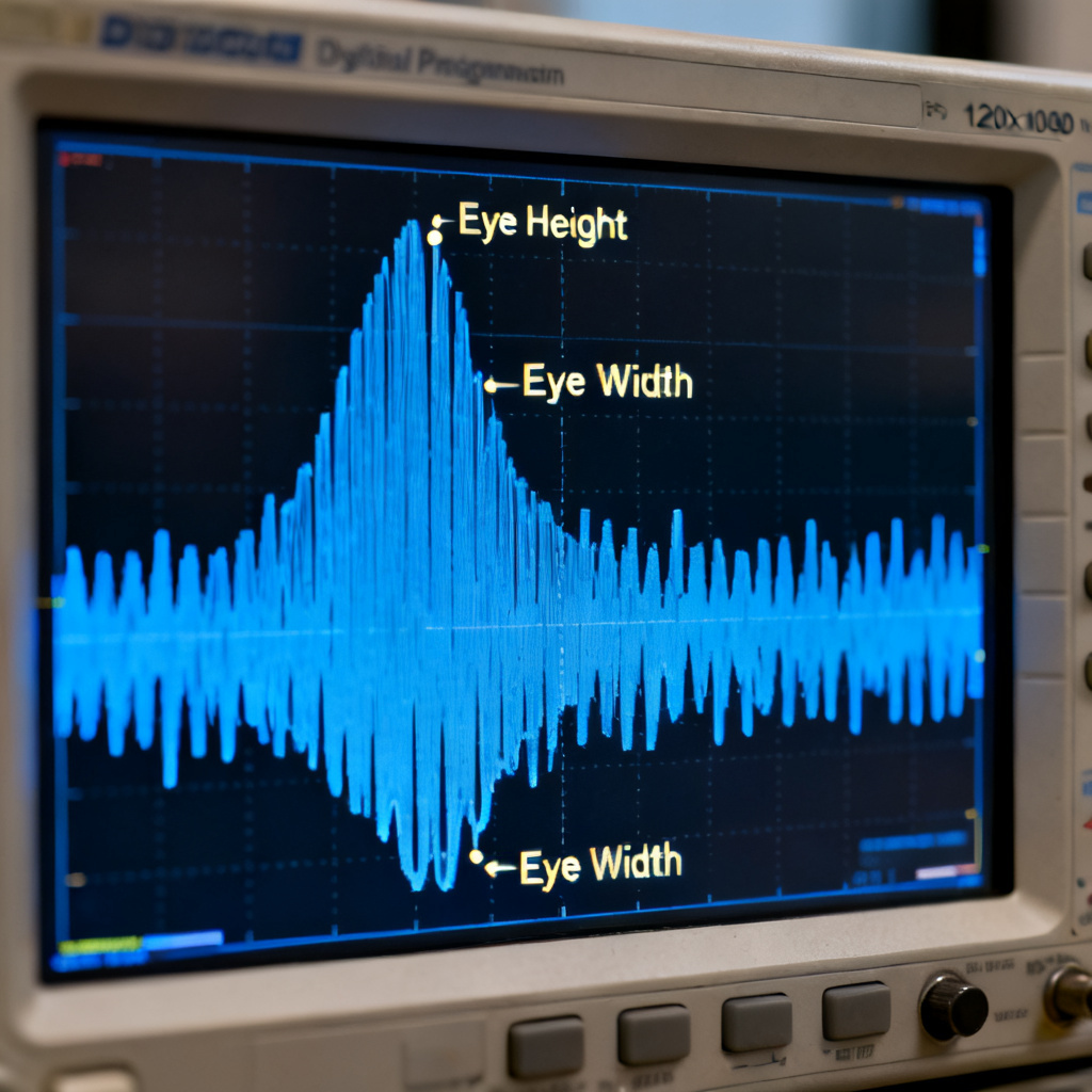
Key metrics include eye height (vertical opening in volts, representing noise margin), eye width (horizontal opening in time, representing timing margin), jitter (horizontal displacement of signal edges), rise time/fall time, overshoot/undershoot, and Bit Error Rate (BER) contour. Jitter is decomposed into random jitter (RJ) from thermal noise and deterministic jitter (DJ) from crosstalk, power supply noise, and impedance mismatches.
2. Setting Up Eye Diagram Analysis in Keysight ADS for Your PCB
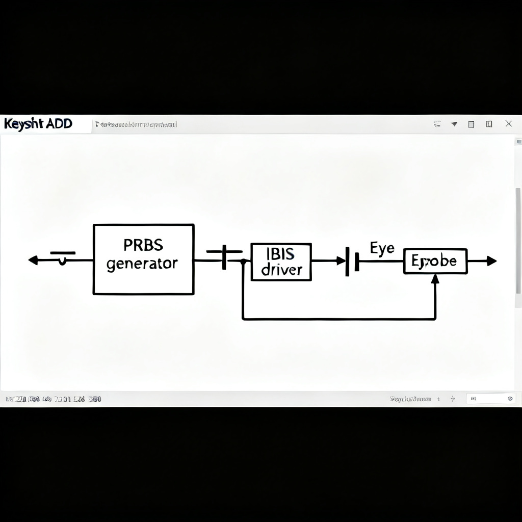
Setting up Eye Diagram PCB analysis in Keysight ADS requires a systematic approach. This section covers the most practical method for PCB designers, from required components to simulation configuration.
2.1 Required Components in the ADS Schematic
To run an eye diagram simulation in ADS, you need a digital stimulus source (PRBS generator with bit rate and amplitude settings), driver model (IBIS model of the transmitter), channel model (PCB trace as transmission line or S-parameter block), receiver model (IBIS model of receiver input), and measurement blocks (Eye Probe at receiver input).
2.2 Configuring the Transient Simulation for Eye Diagram PCB Analysis
Configure the transient simulation controller with a stop time capturing at least 1000-2000 bits, max time step set to 1/20th to 1/50th of the bit period, and appropriate integration method and error tolerance. For a 10 Gbps signal, set max time step to 2-5 ps.
2.3 Running the Simulation and Displaying the Eye Diagram
Run the transient simulation, open the Data Display window, drag the Eye Probe signal, right-click and select Eye Diagram, then configure display parameters in the Eye Diagram Properties dialog.
3. Advanced Analysis and Interpretation in Keysight ADS for Eye Diagram PCB Analysis
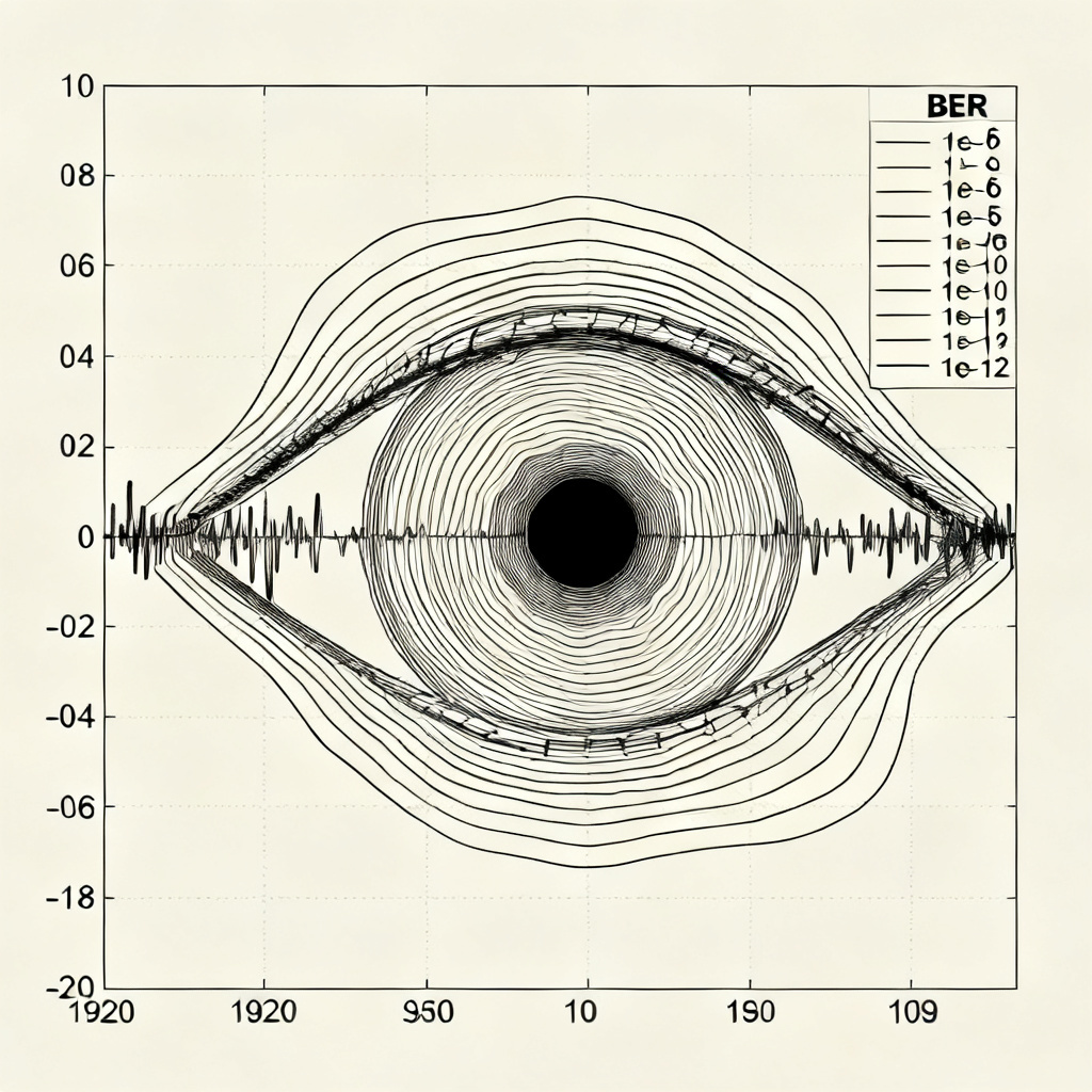
Once the eye diagram is displayed, Keysight ADS provides powerful tools to extract quantitative metrics and diagnose signal integrity problems, including automatic measurement, jitter analysis, BER contour analysis, and statistical eye simulation.
3.1 Automatic Measurement of Eye Parameters
Use the Measure tab or eyeMeasure function to automatically calculate eye height, eye width, jitter (p-p), rise time/fall time, and overshoot/undershoot. Compare these against design specifications such as PCIe Gen4 requiring eye height > 100 mV.
3.2 Jitter Analysis and Decomposition
Use the Jitter Analysis Toolkit to plot TIE vs. time, view jitter histogram, and generate bathtub curve. A Gaussian shape indicates random jitter; a bi-modal shape indicates deterministic jitter.
3.3 BER Contour Analysis
Use the BER Contour function to overlay lines of constant BER on the eye diagram. The innermost contour shows the region with lowest BER, providing the most rigorous verification of channel performance.
3.4 Using Statistical Eye Simulation (Channel Simulator)
For very high-speed designs above 25 Gbps, use ADS Channel Simulator for statistical eye simulation. This method computes the eye diagram mathematically using channel impulse response and supports equalization modeling (CTLE, DFE, FFE).
4. Practical Troubleshooting – Common Issues in Eye Diagram PCB Analysis
| Problem | Eye Diagram Appearance | Likely Cause | ADS Diagnosis & Fix |
|---|---|---|---|
| Eye Closure (Vertical) | Reduced eye height, narrow opening | Excessive loss, attenuation | Check S-parameters (S21). Use thicker copper, wider traces, or low-loss dielectric. Add repeater or equalization. |
| Eye Closure (Horizontal) | Narrow eye width, jitter | Impedance mismatch, reflections | Look for dips in S11 (return loss). Adjust trace width/stackup to achieve 50Ω. Add termination resistors. |
| Double-Edged Eye | Two distinct eye openings | Overshoot, ringing from inductance | Check via stubs, connector parasitics. Use back-drilling or reduce via inductance. |
| Asymmetric Eye | Uneven eye opening | Duty cycle distortion (DCD) | Check driver’s rise/fall time symmetry. Ensure DC blocking caps are properly valued. |
| High Jitter | Blurred edges, wide transition region | Power supply noise, crosstalk | Run crosstalk simulation. Add decoupling capacitors. Increase spacing between traces. |
5. Best Practices for High-Speed PCB Design Using ADS Eye Analysis
For effective Eye Diagram PCB analysis, use realistic IBIS or IBIS-AMI models from chip vendors, include all components (driver, PCB trace, via models, connectors, receiver) with S-parameter models for passive structures, run multiple simulations with varied bit patterns and voltage corners, focus on BER rather than just eye opening, use statistical simulation for long channels above 10 Gbps, and document all results for design reviews and manufacturing handoff.
5.1 Industry Terminology Explained
Signal integrity refers to the quality of electrical signals in a PCB. Jitter is the deviation of signal edges from ideal timing. BER (Bit Error Rate) measures the probability of incorrect bit reception. IBIS (I/O Buffer Information Specification) models accurately represent chip output characteristics. S-parameters describe the frequency-dependent behavior of passive structures like traces and vias.