The eye diagram PCB is the most direct visualization tool for diagnosing signal integrity in high-speed digital channels. This guide explains exactly what the eye diagram reveals about channel loss mechanisms and how equalization restores signal quality.
Eye Diagram PCB Basics: What It Reveals About Channel Health
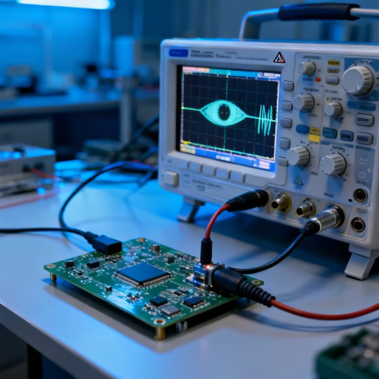
The eye diagram PCB is created by overlaying many bits of a digital signal on an oscilloscope, triggered by a clock recovery circuit. The resulting pattern looks like an open eye. The eye opening (height and width) is a direct measure of signal quality.
Key Parameters of the Eye Diagram
The eye diagram PCB provides several critical metrics for signal integrity analysis. Eye Height (voltage margin) indicates amplitude degradation from loss. Eye Width (timing margin) reveals jitter and timing errors. Rise/Fall Time shows bandwidth limitations. Jitter (random or deterministic) closes the eye horizontally. Mask Margin defines a region the signal must not violate.
How Channel Loss Manifests in the Eye Diagram PCB
Channel loss is the attenuation of signal amplitude and high-frequency content as it travels through the PCB trace, via, connector, and cable. In the eye diagram PCB, loss appears as reduced eye height, slower rise/fall times, increased jitter, and eye closure at the center.
The “Bathtub Curve” and the Eye Diagram PCB
A related concept is the bathtub curve, which plots bit error rate (BER) against sampling point. The eye diagram PCB’s width corresponds to the flat region of the bathtub curve. A closed eye means a narrow flat region, leading to high BER.
Channel Loss Manifestations in the Eye Diagram PCB
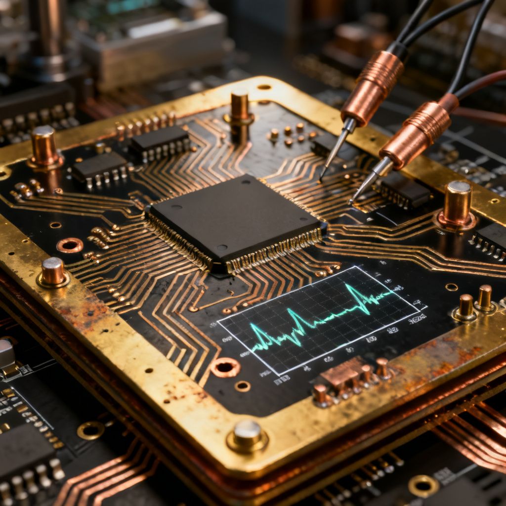
Understanding how specific loss mechanisms appear in the eye diagram PCB is essential for diagnosis. Skin effect causes frequency-dependent attenuation and deterministic jitter. Dielectric loss slows edge rates and creates asymmetric eye opening. Impedance discontinuities produce overshoot, undershoot, and ringing. Crosstalk increases noise floor and reduces eye height.
Skin Effect and the Eye Diagram PCB
At high frequencies, current flows only on the surface of the conductor. This increases resistance proportional to √f. In the eye diagram PCB, skin effect causes frequency-dependent attenuation and increased deterministic jitter.
Dielectric Loss and the Eye Diagram PCB
PCB substrate materials have a loss tangent (tan δ). As frequency increases, the dielectric absorbs energy, causing additional attenuation. In the eye diagram PCB, this appears as slower edge rates and asymmetric eye opening.
Impedance Discontinuities and the Eye Diagram PCB
Any change in impedance causes reflections. In the eye diagram PCB, reflections appear as overshoot/undershoot, ringing, and negative pulses that close the eye.
Crosstalk and the Eye Diagram PCB
Adjacent traces couple energy into the victim line. In the eye diagram PCB, crosstalk appears as increased noise floor and reduced eye height.
Equalization Verification Using the Eye Diagram PCB
The eye diagram PCB is the primary tool to verify if equalization is working. Continuous-Time Linear Equalizer (CTLE) boosts high-frequency content. Decision Feedback Equalizer (DFE) cancels post-cursor ISI. Feed-Forward Equalizer (FFE) pre-distorts the signal at the transmitter.
CTLE and the Eye Diagram PCB
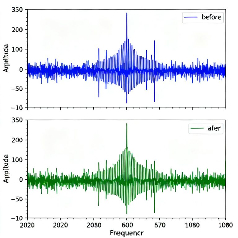
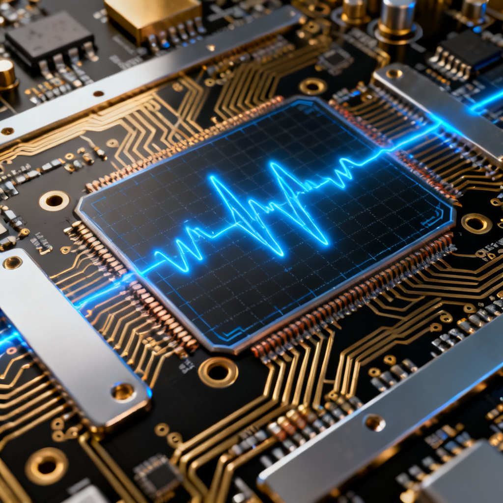
Before CTLE, the eye diagram PCB shows a closed eye with small height and high jitter. After CTLE, the eye height increases, rise/fall times become faster, and deterministic jitter is reduced.
DFE and the Eye Diagram PCB
Before DFE, the eye diagram PCB may show residual ghost traces from post-cursor ISI. After DFE, the eye becomes cleaner and the horizontal opening widens.
FFE and the Eye Diagram PCB
At the transmitter, the eye diagram PCB may look over-equalized with pre-emphasis. At the receiver, the eye is more open than without FFE.
The “Eye Opening” as a Metric for Equalizer Tuning
Engineers use the eye diagram PCB to tune equalizer parameters. CTLE gain is swept to maximize eye height. DFE tap weights are adjusted to minimize the post-cursor tail. FFE pre-emphasis is optimized to flatten the channel response.
Practical PCB Design Implications from the Eye Diagram PCB
The eye diagram PCB directly guides material selection, trace length, via stub management, and connector design. Material selection for low-loss substrates is critical when the eye shows dielectric loss. Trace length must be reduced for higher data rates. Via stub management using back-drilling improves eye opening. Connector and cable effects must be isolated using de-embedding.
Material Selection Based on Eye Diagram PCB
If the eye diagram PCB shows severe dielectric loss, consider low-loss materials like Megtron 6 or Rogers 4350B for >10 Gbps long traces.
Trace Length and Routing from Eye Diagram PCB
The eye diagram PCB directly correlates with trace length. At 10 Gbps, a 10-inch trace on FR4 will show a closed eye; a 2-inch trace will show an open eye.
Via Stub Management Using Eye Diagram PCB
Via stubs create impedance discontinuities that close the eye. The eye diagram PCB after back-drilling will show reduced overshoot and wider horizontal opening.
Connector and Cable Effects in Eye Diagram PCB
If the eye diagram PCB shows a knee or notch at a specific frequency, suspect a connector or cable resonance.
Advanced Eye Diagram PCB Analysis for Equalization
Advanced analysis includes PAM4 vs. NRZ eye diagrams, statistical vs. measured eyes, and eye diagram and BER relationships.
PAM4 vs. NRZ Eye Diagrams
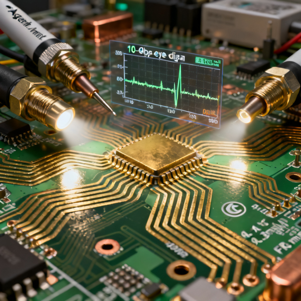
NRZ has one eye opening. PAM4 has three stacked eye openings. Loss causes the three eyes to have different heights. Equalization is critical to make all three eyes equally open.
Statistical Eye vs. Measured Eye
The statistical eye is generated from channel S-parameters and equalizer models. The measured eye is from actual hardware. The difference indicates manufacturing tolerances.
Eye Diagram PCB and BER
A closed eye does not always mean a failed link. Forward error correction (FEC) can recover data even with a partially closed eye. However, the eye diagram PCB tells you how much margin you have.
FAQ: Eye Diagram PCB and Equalization
What does a closed eye diagram PCB indicate?
A closed eye diagram PCB indicates significant channel loss, high jitter, or impedance discontinuities that degrade signal quality. Equalization may be needed to restore the eye opening.
How does equalization improve the eye diagram PCB?
Equalization compensates for channel loss by boosting high frequencies (CTLE), canceling ISI (DFE), or pre-distorting the signal (FFE), resulting in a more open eye diagram PCB.
What is the relationship between eye diagram PCB and BER?
The eye diagram PCB width corresponds to the flat region of the bathtub curve. A wider eye opening means lower bit error rate (BER) and more timing margin.
Can the eye diagram PCB predict equalizer settings?
Yes, engineers use the eye diagram PCB to tune CTLE gain, DFE tap weights, and FFE pre-emphasis by measuring eye height and width changes.
Why is the eye diagram PCB important for high-speed PCB design?
The eye diagram PCB provides a direct visual representation of signal integrity, allowing designers to identify loss mechanisms, verify equalization, and optimize PCB layout for reliable data transmission.
| Eye Diagram PCB Parameter | What It Indicates | Channel Loss Manifestation |
|---|---|---|
| Eye Height | Voltage margin | Reduced by skin effect and dielectric loss |
| Eye Width | Timing margin | Narrowed by jitter and ISI |
| Rise/Fall Time | Bandwidth limitation | Slowed by frequency-dependent loss |
| Jitter | Timing uncertainty | Increased by reflections and crosstalk |
| Mask Margin | Signal quality compliance | Violated when loss is excessive |
| Equalization Type | Function | Eye Diagram PCB Improvement |
|---|---|---|
| CTLE | High-frequency boost | Increased eye height, faster edges |
| DFE | Post-cursor ISI cancellation | Cleaner eye, wider horizontal opening |
| FFE | Pre-distortion at transmitter | More open eye at receiver, reduced noise |
Why Choose Our High-Speed PCB Manufacturing?
We specialize in low-loss materials (Megtron 6, Rogers, PTFE), precision impedance control (±5%), back-drilling for via stub removal, and design-for-signal-integrity consultation. Our engineering team helps you achieve an open eye diagram PCB at any data rate. Contact us today to discuss your high-speed PCB project.