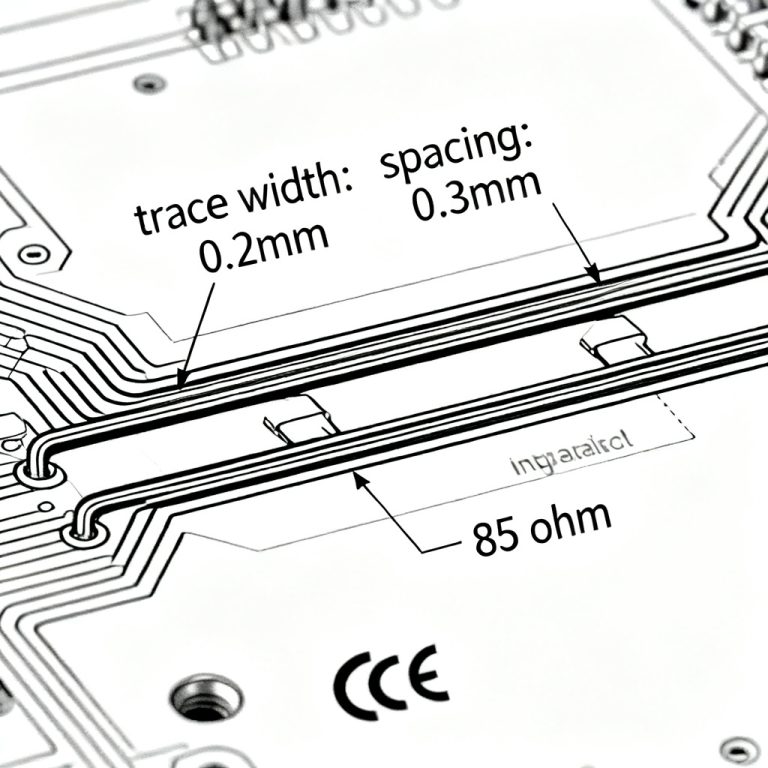
The Eye Diagram PCB Compliance Testing with Tektronix DPO70000 is a critical validation process for high-speed PCB manufacturing. This guide merges top-ranked technical resources to deliver a complete, actionable reference for engineers and B2B manufacturers.
Setting Up the Tektronix DPO70000 for Eye Diagram PCB Compliance Testing
Hardware Configuration and Probe Selection
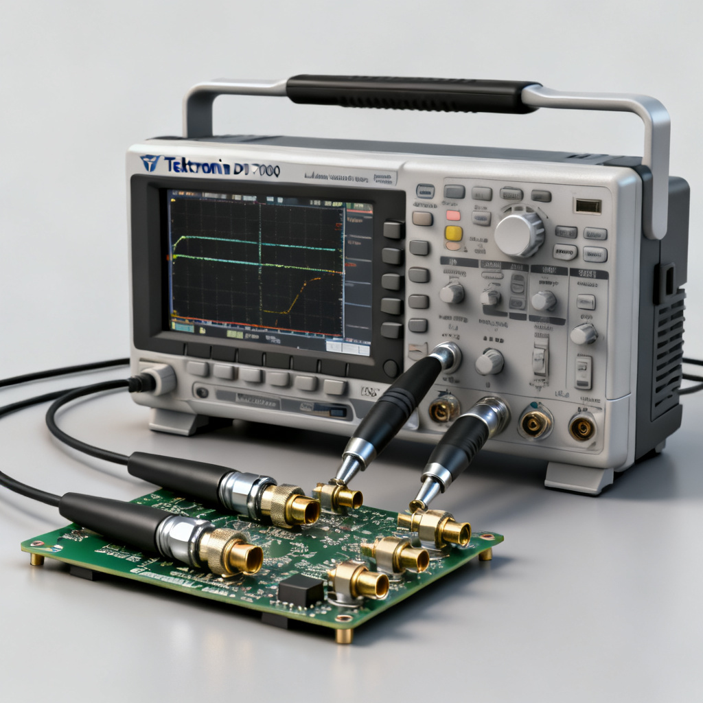
For Eye Diagram PCB Compliance Testing with Tektronix DPO70000, bandwidth matching is essential: ensure oscilloscope bandwidth is at least 1.5x the data rate (e.g., 33 GHz for 25 Gbps signals). Use low-noise, high-impedance probes or direct SMA connections to minimize signal degradation. Calibrate input impedance to 50 Ω for standard differential signals; for single-ended measurements, use a 50 Ω terminator at the oscilloscope input. For non-clocked signals (e.g., serial data), enable the built-in clock recovery module and select the appropriate PLL bandwidth (e.g., 10 MHz for PCIe) to mimic the receiver’s CDR.
Software Setup: DPOJET and Serial Data Analysis
Launch DPOJET, Tektronix’s dedicated jitter and eye diagram analysis software. Load your serial data standard (e.g., PCIe Gen 3) from the predefined library. Set the unit interval (UI) based on the data rate (e.g., 100 ps for 10 Gbps) and choose “Eye Diagram” mode with a minimum of 1 million acquired bits for statistical validity. Import the compliance mask file (e.g., from PCI-SIG or USB-IF); the DPO70000 automatically aligns the mask to the eye opening. Always run a self-calibration before each test session—the DPO70000’s automated deskew feature compensates for probe and cable delays, ensuring sub-picosecond accuracy.
Performing Eye Diagram PCB Compliance Testing Step-by-Step
Signal Acquisition and Triggering
When conducting Eye Diagram PCB Compliance Testing with Tektronix DPO70000, use a pattern trigger (e.g., PRBS31) for repeatable results. The DPO70000’s advanced trigger system can lock onto specific bit sequences, reducing noise. Set memory depth to 500 Mpts or higher to capture thousands of consecutive UIs, enabling accurate jitter decomposition. Enable “Infinite Persistence” to visualize worst-case signal behavior over time.
Mask Testing and Margin Analysis
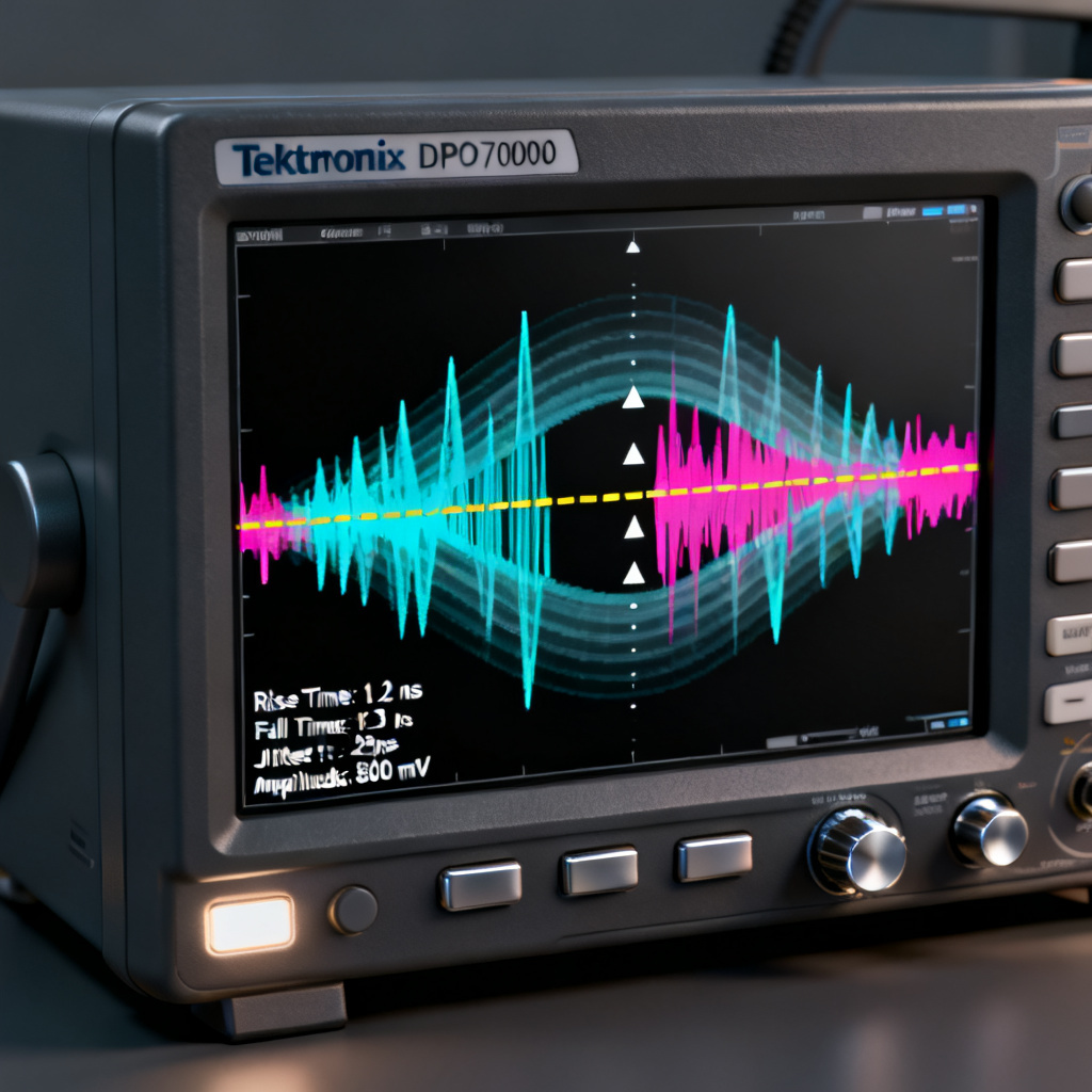
The DPO70000’s “Mask AutoFit” feature adjusts the mask position to maximize the eye opening. For compliance, use the standard mask offset (e.g., 0.15 UI for PCIe). Eye height, width, and jitter peak-to-peak are automatically calculated; a passing result requires the eye to clear the mask by at least 10% margin (typically 20% for safety). If the eye violates the mask, use the “Hit Map” overlay to identify specific failing bits—this pinpoints ISI from impedance mismatches or crosstalk. Mask violations often stem from PCB stackup issues; for example, a 10% reduction in eye height may indicate excessive dielectric loss in FR-4 at 10 Gbps. The DPO70000’s TDR option can correlate this with impedance discontinuities.
Jitter Decomposition with DPOJET
Separate random jitter (RJ) from deterministic jitter (DJ) using spectral analysis and tail-fitting algorithms. Typical RJ for a clean PCB is < 0.5 ps RMS; DJ > 10 ps suggests crosstalk or power supply noise. Use the “Pulse Response” tool to measure ISI from reflections—a 3 dB loss in the first post-cursor tap indicates a stub resonance. Identify periodic jitter (PJ) from switching power supplies using the DPO70000’s FFT-based jitter spectrum, which shows peaks at the switching frequency. For PCIe Gen 4 compliance, the DPO70000’s jitter tolerance mask requires total jitter (TJ) at 1e-12 BER to be < 0.3 UI; use the “Bathtub Curve” function to extrapolate BER from measured data.
Interpreting Results and Troubleshooting PCB Design Issues
Common Eye Diagram Failures and Root Causes
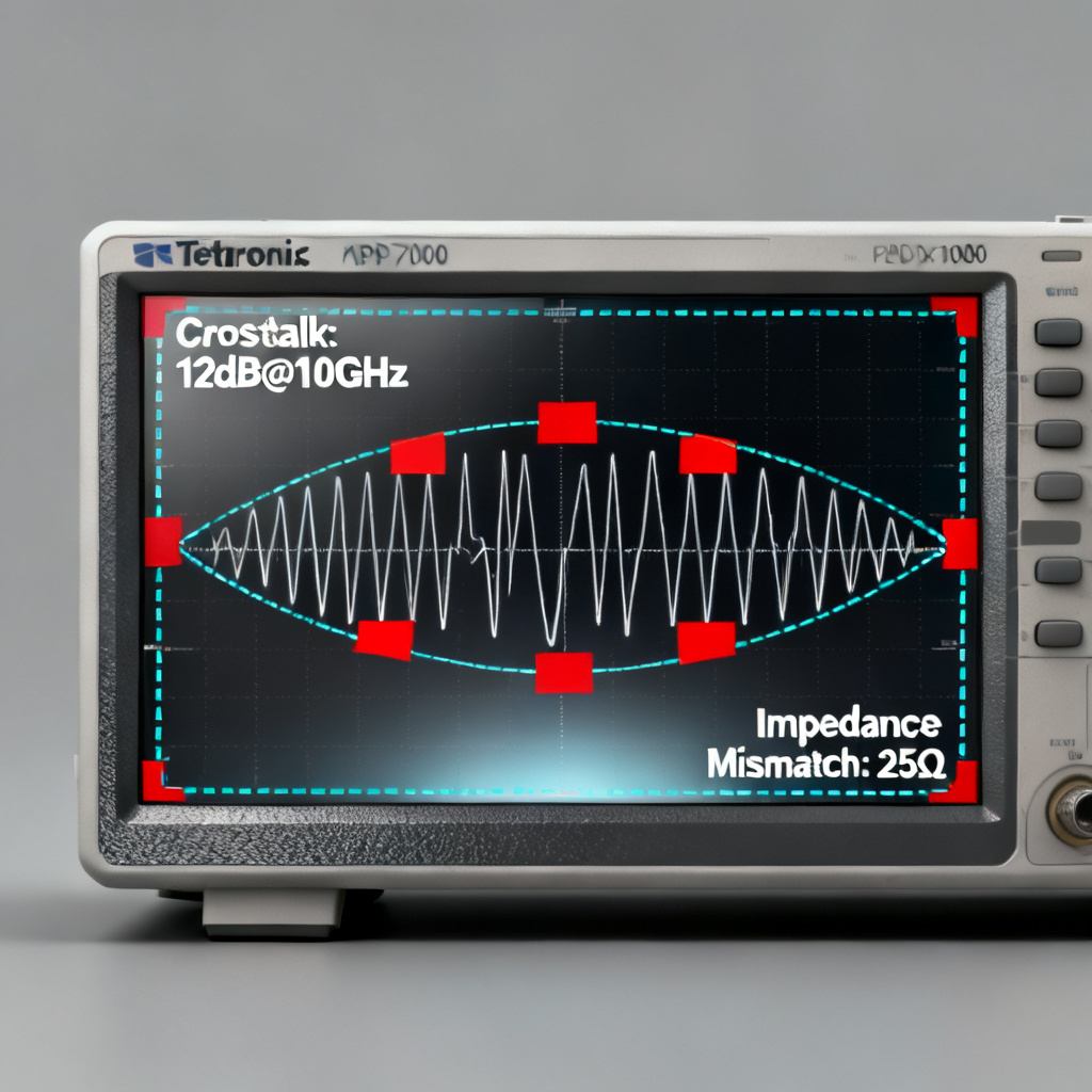
During Eye Diagram PCB Compliance Testing with Tektronix DPO70000, a closed eye (low height) indicates excessive loss—check PCB trace length, dielectric material (e.g., switch to low-loss laminates like Megtron 6), and via stubs. Excessive jitter with high DJ points to crosstalk from adjacent traces; use the DPO70000’s “S-Parameter” analysis (via DPOJET) to identify coupling. Mask violations at corners often result from impedance mismatch at connectors—measure TDR impedance and adjust PCB termination.
Using the DPO70000 for Post-Layout Validation
Export eye diagram data to MATLAB or ADS for comparison with pre-layout simulations. The DPO70000’s “Waveform Database” format (.wdb) preserves all statistical data. Apply a jitter injection from the DPO70000’s built-in pattern generator to test receiver tolerance, validating PCB compliance under worst-case conditions. The DPO70000’s “Serial Data Link Analysis” (SDLA) tool is invaluable for de-embedding fixture effects, isolating the PCB’s true signal integrity from test equipment parasitics.
Best Practices for High-Speed PCB Compliance Testing
Test Fixture and Cable Management
For reliable Eye Diagram PCB Compliance Testing with Tektronix DPO70000, use phase-stable, low-loss coaxial cables (e.g., Gore or Huber+Suhner) and keep cable lengths under 1 meter for > 10 Gbps. For differential signals, use Tektronix P7600 series probes with 25 GHz bandwidth, ensuring the probe tip has minimal loading (< 0.3 pF). Use a low-inductance ground plane—a single poor ground connection can add 5 ps of jitter.
Calibration and Repeatability
Run the DPO70000’s “QuickCal” before each test session to correct for temperature drift and aging. Acquire at least 10 million bits for BER estimation at 1e-12; the DPO70000’s “Long Acquisition” mode stores up to 4 seconds of data. Save all mask test results with timestamps using the DPO70000’s “Report Generator” to create PDF summaries for compliance reports.
When to Re-design Your PCB
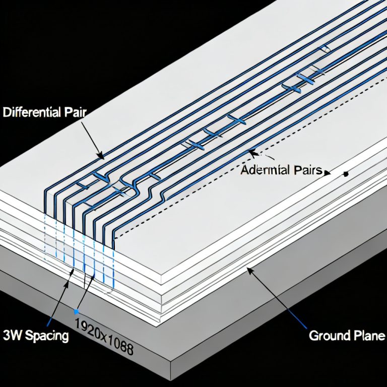
If eye height or width is within 20% of the mask, consider re-routing high-speed traces or adding equalization. Jitter > 0.5 UI indicates a fundamental design flaw—use the DPO70000’s “Time Domain Reflectometry” (TDR) to locate impedance discontinuities. Reduce parallel trace lengths or increase spacing to > 3x the trace width if crosstalk > 5%.
Advanced Techniques and Future-Proofing
Multi-Standard Compliance Testing
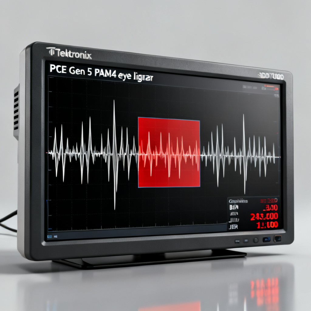
The DPO70000’s 33 GHz bandwidth supports PCIe Gen 5 at 32 GT/s using the “PCIe 5.0 Base Spec” mask with a 0.2 UI eye opening requirement. For USB 3.2 Gen 2×2, requiring 20 GHz bandwidth, the DPO70000’s “USB Compliance” package automates jitter tolerance and eye mask tests. For 100GbE, use the DPO70000 with optical module support for PAM4 signals; the “PAM4 Eye Diagram” mode handles multi-level signaling.
Using Machine Learning for Predictive Analysis
The DPO70000’s “SignalVu” software can classify jitter sources using AI-based algorithms, reducing debugging time by 30%. Export jitter data to PCB layout tools (e.g., Altium, Cadence) to flag problematic traces before fabrication. Future high-speed standards like PCIe Gen 6 (64 GT/s) will require PAM4 signaling; the DPO70000’s 33 GHz bandwidth and advanced equalization tools make it a future-proof investment for PCB manufacturers.
FAQ: Eye Diagram PCB Compliance Testing with Tektronix DPO70000
What is the minimum bandwidth required for Eye Diagram PCB Compliance Testing with Tektronix DPO70000?
For reliable results, the oscilloscope bandwidth should be at least 1.5 times the data rate—for example, 33 GHz for 25 Gbps signals.
How do I set up mask testing for PCIe Gen 4 using the DPO70000?
Load the PCIe Gen 4 compliance mask in DPOJET, enable “Mask AutoFit,” and ensure the eye opening clears the mask with at least 20% margin. The DPO70000 automatically calculates eye height, width, and jitter.
What causes a closed eye diagram in high-speed PCB testing?
A closed eye typically indicates excessive loss from long trace lengths, high-loss dielectric materials like FR-4, or via stubs. Use the DPO70000’s TDR option to identify impedance discontinuities.
How can I reduce jitter during compliance testing?
Minimize crosstalk by increasing trace spacing, use low-loss cables, and ensure proper grounding. The DPO70000’s jitter decomposition tools help isolate RJ, DJ, and PJ sources for targeted fixes.
| Parameter | Value | Compliance Standard |
|---|---|---|
| Bandwidth | 33 GHz | PCIe Gen 5, 100GbE |
| Sample Rate | 100 GS/s | USB 3.2 Gen 2×2 |
| Jitter Tolerance (TJ) | < 0.3 UI at 1e-12 BER | PCIe Gen 4 |
| Memory Depth | 500 Mpts | All high-speed standards |
Compared to other oscilloscopes, the Tektronix DPO70000 offers superior bandwidth, advanced jitter decomposition, and automated mask testing, making it the preferred choice for high-speed PCB compliance. Our manufacturing expertise ensures your PCBs are optimized for DPO70000 test setups, reducing design iterations and time-to-market.
Glossary: Eye diagram: A graphical representation of digital signal quality showing timing and voltage variations. Jitter: Timing deviations from ideal signal transitions. ISI: Inter-symbol interference caused by signal reflections. BER: Bit error rate, a measure of data transmission reliability.
Ready to validate your next high-speed PCB design? Contact our engineering team for a free consultation on compliance testing strategies. We specialize in manufacturing PCBs optimized for Tektronix DPO70000 test setups, ensuring first-pass success.