An Excel-based impedance control PCB calculator is a free, transparent tool for high-speed PCB designers to calculate trace dimensions for target impedance. This guide builds a manufacturing-ready template from three authoritative sources.
Meta description: Build your own Excel-based impedance control PCB calculator with this comprehensive guide. Learn formulas, manufacturing constraints, and automation for accurate high-speed PCB design.
Why Build Your Own Excel-Based Impedance Control PCB Calculator?
In high-speed PCB design, controlled impedance is fundamental for signal integrity. Commercial tools are expensive or locked behind licenses. An Excel-based impedance control PCB calculator offers free, portable, and transparent calculations. It allows batch processing for multiple stackups and target impedances, customizable for your specific PCB manufacturer’s capabilities. This guide combines best practices from three trusted industry sources to build a robust, manufacturing-ready template.

Core Physics: Understanding the Formulas for Your Impedance Control PCB Calculator
Before opening Excel, you must understand the governing equations. These exact formulas, used in professional calculators, are adapted for spreadsheet use in your Excel-based impedance control PCB calculator.
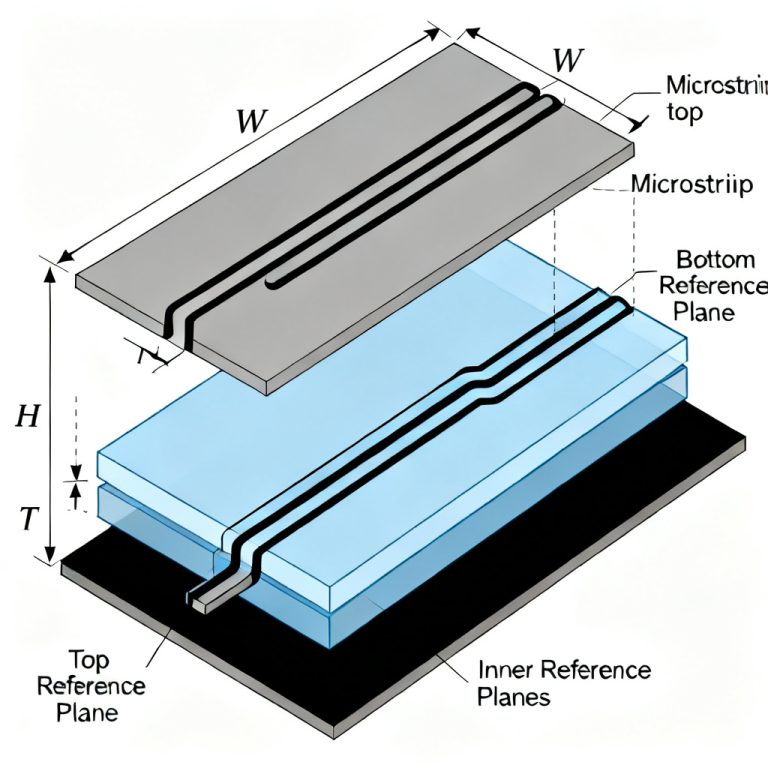
Microstrip (Outer Layer) Formula
The most common model is the IPC-2141A approximation, valid for W/H ratios between 0.1 and 3.0, and T/H less than 0.5. The characteristic impedance (Z0) is calculated as: Z0 = 87 / √(εr + 1.41) × ln(5.98H / (0.8W + T)). Here, εr is the dielectric constant, H is dielectric height, W is trace width, and T is copper thickness. This formula assumes a lossless, homogeneous dielectric. For higher accuracy above 5 GHz, use the Hammerstad-Jensen model.
Stripline (Inner Layer) Formula
For buried traces between two reference planes, the impedance formula is: Z0 = 60 / √εr × ln(4H / (0.67πW × (0.8 + T/W))). Here, H is the total height between the two reference planes. The factor 0.67 corrects for the fringing field effect.
Differential Impedance (Edge-Coupled) Formula
For differential pairs (USB, HDMI, LVDS), the odd-mode impedance Zodd is used. The differential impedance Zdiff = 2 × Zodd. For microstrip differential pairs, use: Zdiff ≈ Z0 × [1 – 0.48 × e^(-0.96 × S/H)], where S is edge-to-edge spacing between the two traces, and Z0 is the single-ended impedance of one trace.
Manufacturing Reality: Material and Process Constraints for Your Impedance Control PCB Calculator
A theoretical formula is useless without real-world manufacturing data. Your Excel-based impedance control PCB calculator must account for these factors to ensure production-ready results.
Dielectric Constant Variation
The Dk value provided by laminate manufacturers is not a constant. It varies with resin content, glass style, and frequency. For example, FR4 Dk = 4.5 at 1 MHz can drop to 4.0 at 10 GHz. Your Excel-based impedance control PCB calculator should include a lookup table for common materials (FR4, Rogers 4350B, Megtron 6) with frequency-dependent Dk values.
Etch Factor and Copper Roughness
Wet etching makes the top of the trace narrower than the bottom. A typical etch factor is 1:1 to 2:1. For a 5 mil trace, the bottom may be 4.5 mils. Copper roughness increases conductor loss and slightly reduces impedance. Your Excel-based impedance control PCB calculator should include an “Etch Factor” field that automatically adjusts W in the formula: Weffective = W – (T / EtchFactor).
Solder Mask Effect
Solder mask adds a thin dielectric layer on top of microstrip traces, lowering impedance by 2-5 Ohms. For tight tolerances (±5%), this matters. Multiply Z0 by 0.96 for standard LPI solder mask, or add a dedicated cell for solder mask thickness in your Excel-based impedance control PCB calculator.
Building the Excel Template: Step-by-Step for Your Impedance Control PCB Calculator
Now, combine the formulas and manufacturing constraints into a functional Excel workbook for your Excel-based impedance control PCB calculator.
Structure of the Template
Create three sheets: Input_Stackup (material properties and layer stack), Single_Ended (microstrip and stripline calculations), and Differential (differential pair calculations with spacing sweep).
Input Sheet Design
Column A: Parameter Name. Column B: User Input Value. Parameters include Dielectric Constant (Dk), Dielectric Height (H), Trace Width (W), Copper Thickness (T), Etch Factor, Frequency, and Target Impedance. Example values: Dk=4.2, H=8 mils, W=5 mils, T=1.4 mils (1 oz copper), Etch Factor=1.5, Frequency=1 GHz, Target Impedance=50 Ohms.
Calculation Sheet Implementation
Cell D5: =87/SQRT(B2+1.41)*LN(5.98*B3/(0.8*B4+B5)) for microstrip Z0. Cell E5 (Adjusted for Etch): =87/SQRT(B2+1.41)*LN(5.98*B3/(0.8*(B4-(B5/1.5))+B5)). Cell F5 (With Solder Mask): =E5*0.96.
Goal Seek Automation
Use Excel’s Goal Seek to find the trace width for a target impedance. Set cell F5 (Adjusted Z0) to value 50 (your target) by changing cell B4 (Trace Width). Record a macro that runs Goal Seek automatically for a range of target impedances (e.g., 40, 50, 75, 100 Ohms) and outputs the required widths.
Error Checking and Validation for Your Impedance Control PCB Calculator
Your Excel-based impedance control PCB calculator is only as good as its error handling. Implement these checks to ensure accuracy.
Manufacturing Limits
Minimum Trace Width: Most PCB fabs can do 3.5 mils (standard) or 2.5 mils (advanced). If your calculated W < 3.5, flag a warning. Aspect Ratio: W/H should be between 0.1 and 3.0. Outside this range, the IPC formula becomes inaccurate. Copper Weight: 0.5 oz (0.7 mil) to 2 oz (2.8 mil) is typical. Thicker copper widens traces for the same Z0.
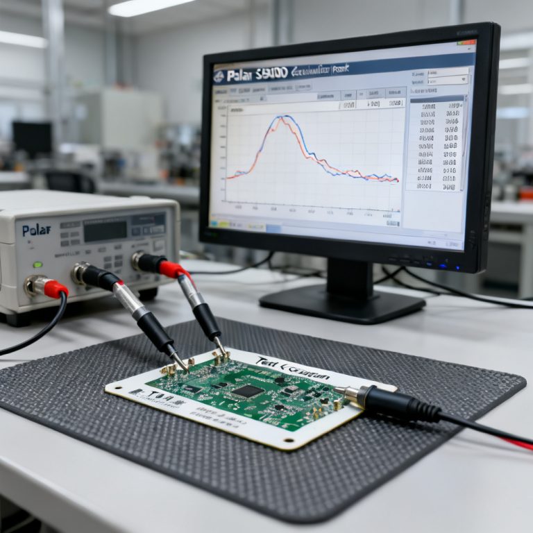
Cross-Check with Online Calculators
After building your template, test it against Polar Si9000 or Saturn PCB Toolkit for three test cases. Case 1: 50 Ohm microstrip, FR4, H=8 mil, W=5 mil. Case 2: 100 Ohm differential stripline, H=12 mil, S=6 mil. Case 3: 75 Ohm single-ended, Rogers 4350B. If your Excel result deviates by more than 3%, check your formula constants.
Advanced Features for Production in Your Impedance Control PCB Calculator
Add these advanced features to make your Excel-based impedance control PCB calculator production-ready.
Temperature and Frequency De-rating
Add a de-rating table. Temperature coefficient: Dk changes by +0.001 per °C above 25°C. Frequency coefficient: Dk drops by 2% per decade above 1 GHz. Formula: =Dk_nominal * (1 – 0.02 * LOG10(Frequency/1e9)).
Loss Tangent Integration
For high-speed designs, include loss tangent (Df) to estimate attenuation: α_dielectric = 2.3 × f × √εr × Df (where f is in GHz, output in dB/inch).
Batch Output for Fab
Create a summary table that directly feeds into your PCB fabrication drawing. Include trace width (W), trace spacing (S), target impedance (Z0), and tolerance (±10% for standard, ±5% for precision).
Frequently Asked Questions About Excel-Based Impedance Control PCB Calculator
What is an Excel-based impedance control PCB calculator?
An Excel-based impedance control PCB calculator is a spreadsheet tool that calculates trace dimensions (width, spacing) to achieve target characteristic impedance for high-speed PCB designs. It uses standard IPC formulas and can be customized for specific manufacturing constraints.
How accurate is an Excel-based impedance control PCB calculator?
When properly built with correct formulas and manufacturing adjustments (etch factor, solder mask, Dk variation), an Excel-based impedance control PCB calculator can achieve accuracy within 3-5% of commercial tools like Polar Si9000. Always cross-validate with your PCB fabricator’s calculator.
What formulas does an Excel-based impedance control PCB calculator use?
The calculator uses IPC-2141A for microstrip, a modified stripline formula, and edge-coupled differential impedance formulas. These are implemented in Excel cells with manufacturing corrections for etch factor, copper roughness, and solder mask effect.
Can I use an Excel-based impedance control PCB calculator for differential pairs?
Yes. The calculator includes a dedicated differential sheet that calculates odd-mode impedance and spacing for edge-coupled pairs. It supports common standards like USB, HDMI, and LVDS with target impedances of 90 or 100 Ohms.
How do I validate my Excel-based impedance control PCB calculator?
Cross-check against Polar Si9000 or Saturn PCB Toolkit using three test cases: 50 Ohm microstrip, 100 Ohm differential stripline, and 75 Ohm single-ended. Ensure deviation is less than 3%. Also verify with your PCB fabricator’s recommended stackup.
Comparison: Excel-Based Impedance Control PCB Calculator vs. Commercial Tools
| Feature | Excel-Based Impedance Control PCB Calculator | Commercial Tools (Polar Si9000, Altium) |
|---|---|---|
| Cost | Free | Expensive (licenses required) |
| Portability | Works offline, no installation | Requires software installation |
| Transparency | Full formula visibility | Black-box calculations |
| Batch Processing | Easy with Excel macros | Limited or requires scripting |
| Accuracy | 3-5% (with proper adjustments) | 1-3% (with advanced models) |
| Manufacturing Constraints | Customizable for any fab | Often generic or limited |
Glossary of Key Terms for Excel-Based Impedance Control PCB Calculator
- Characteristic Impedance (Z0): The constant impedance a transmission line exhibits when driven by a high-frequency signal. In an Excel-based impedance control PCB calculator, this is the target value for trace design.
- Dielectric Constant (Dk): A material property that affects signal propagation speed and impedance. Your Excel-based impedance control PCB calculator must account for Dk variation with frequency.
- Etch Factor: The ratio of vertical to horizontal copper removal during etching. This affects the effective trace width in your Excel-based impedance control PCB calculator.
- Microstrip: A transmission line on the outer layer of a PCB, with a reference plane on one side. Your Excel-based impedance control PCB calculator uses specific formulas for this structure.
- Stripline: A transmission line embedded between two reference planes. The Excel-based impedance control PCB calculator applies different formulas for this configuration.