Article Summary
Most hardware engineers and procurement managers make a common mistake: calculating high speed pcb prototype cost simply by multiplying bulk unit price by quantity. Unlike mass production, high-speed PCB prototypes carry heavy one-time engineering, stackup design, impedance simulation and setup fees that must be spread over only 1–10 boards. This comprehensive guide to high speed pcb prototype cost covers full cost structure, layer-based price ranges, premium for high-speed materials, hidden extra charges, rush order pricing, and actionable strategies to cut your prototype budget without sacrificing signal integrity and performance.
1. How Much Does a High-Speed PCB Prototype Cost?
If you are budgeting for 4-layer to 10-layer high-speed PCB prototypes for R&D, sample validation and pre-production testing, you need to abandon the regular bulk pricing logic. As detailed in the high-speed PCB cost master page, understanding high speed pcb prototype cost requires a different framework than mass production.
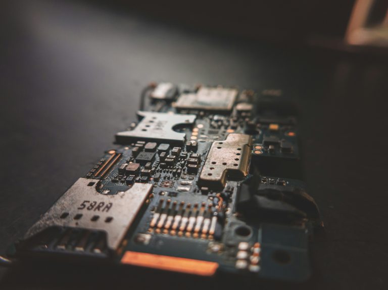
High-speed PCB design involves complex pre-production work: stackup optimization, impedance modeling, high-speed signal integrity checking, DFM review and CAM file preparation. These fixed one-time engineering and setup expenses account for a large share of the total order cost. When you only order 1 to 10 prototype pieces, these fixed fees cannot be diluted, making per-piece prototype cost far higher than mass-production unit price.
Many overseas buyers and junior designers underestimate high speed pcb prototype cost because they ignore fixed engineering overhead, special high-speed material premiums, and extra charges for impedance control, backdrilling and tight tolerance requirements.
This guide integrates real manufacturing cost data, industry standard price ranges, and insider cost optimization experience from top global PCB manufacturers. It helps you set a realistic budget, understand every cost driver, and avoid unnecessary overspending on your next high-speed PCB prototype project.
2. Full High-Speed PCB Prototype Cost Breakdown
The total high speed pcb prototype cost consists of five core components, with engineering and tooling fees dominating small-run orders. For PCB Manufacturing, understanding this breakdown is essential for budget planning.
| Cost Component | Percentage | Description |
|---|---|---|
| Engineering & Tooling Fee | 30–50% | CAM data processing, stackup design, impedance simulation, DFM checking, production line setup |
| Material Cost | 20–30% | Substrate laminate, copper foil, prepreg, solder mask, surface finish |
| Manufacturing Operation Cost | 15–25% | Line changeover, precision lamination, controlled impedance etching, specialized drilling |
| Testing Fee | 5–10% | Flying probe testing, impedance verification, continuity testing, TDR validation |
| Management, QC & Profit | 5–10% | Project management, quality inspection, logistics, manufacturer overhead |
Engineering and tooling fee is the largest cost portion, especially for complex designs at 10Gbps+ or 5G millimeter-wave applications. When you calculate high speed pcb prototype cost, remember that fixed fees dominate small-run orders.
3. Typical Prototype Pricing: 1–10 Pieces by Layers & Materials
For the most common prototype quantity of 1–10 units, high speed pcb prototype cost varies significantly based on layer count and PCB material grade. More layers mean higher stackup complexity, lower production yield and higher overall cost.
3.1 Standard FR4 & High-Tg FR4 Pricing
| Layer Count | Standard FR4 | High-Tg FR4 |
|---|---|---|
| 4 Layer | $200–400 | $250–500 |
| 6 Layer | $350–700 | $400–850 |
| 8 Layer | $600–1100 | $700–1300 |
| 10 Layer | $900–1700 | $1000–2000 |
Standard FR4 fits basic moderate-speed circuits, while high-Tg FR4 is necessary for designs with high thermal stress. Every additional 2 layers usually increase total high speed pcb prototype cost by 30–50%.
3.2 High-Speed Low-Loss Material Pricing
For 5G, RF, 10Gbps/25Gbps serial links and millimeter-wave applications, standard FR4 cannot meet requirements. For detailed material data, see High-Speed PCB Material.
| Material Classification | Representative Grade | 4-Layer Price | 8-Layer Price |
|---|---|---|---|
| Mid-Loss | S7000 / FR408 | $300–600 | $800–1600 |
| Low-Loss | Megtron 6 / RO4350B | $400–800 | $1100–2200 |
| Ultra-Low-Loss | Megtron 8 / RO5880 | $500–1000 | $1500–3000 |
Mid-loss materials suit general high-speed digital designs; low-loss options apply to medium-to-high frequency communication; ultra-low-loss laminates are for premium high-speed and millimeter-wave projects, costing 2–4 times more than ordinary FR4. For Impedance Matching, proper material selection is critical.
4. How Order Quantity Allocates Engineering Fees
One-time engineering and setup fees are fixed regardless of order quantity, which directly determines your average high speed pcb prototype cost per board.
| Quantity | Cost Impact | Recommendation |
|---|---|---|
| 1–3 pieces | Highest unit cost | Single-sample R&D validation only |
| 4–10 pieces | Slightly reduced | Moderate cost sharing |
| 10+ pieces | Much better pricing | Engineering cost fully diluted |
| Reorders (unchanged design) | Lowest cost | Engineering fees waived or heavily discounted |
For small batch PCB production and high speed PCB mass production, engineering fees are amortized over larger quantities. If your project timeline allows slightly increasing prototype quantity or combining multiple designs into one panel, you can effectively lower the average high speed pcb prototype cost per design.
5. Hidden & Extra Costs That Raise Prototype Prices
Base prototype pricing only covers standard specifications. Any customized high-speed requirements will trigger additional surcharges, which are often overlooked when estimating high speed pcb prototype cost. For pcb cost factors, these hidden costs are explained in detail.
| Extra Requirement | Cost Premium | Trigger Condition |
|---|---|---|
| Impedance Control | +10–20% | Controlled impedance traces required for high-speed signals |
| Tight Impedance Tolerance | +15–25% | Strict ±7% tolerance instead of standard ±10% |
| Backdrilling Process | +10–20% | 10Gbps+ high-speed links to eliminate stub resonance |
| Non-Standard Special Materials | +30–100% | Uncommon laminates, customized prepreg or exotic finishes |
| Low-Yield Complex Design | +10–20% | High layer count, fine line width and tight spacing |
Besides visible surcharges, hidden costs include special material storage fees, extra TDR impedance testing fees, and rework costs caused by repeated design revisions. Confirm whether your design truly needs these strict requirements to avoid unnecessary high speed pcb prototype cost waste.
6. Quick-Turn High-Speed PCB Prototype Rush Pricing
R&D projects often require fast delivery. Rush production rearranges production schedules, prioritizes material allocation and compresses testing cycles. For quick turn pcb service, clear tiered surcharges apply:
| Rush Service | Premium Rate | Impact on High Speed PCB Prototype Cost |
|---|---|---|
| 24h Quick-Turn | +100–200% | Total cost nearly doubled |
| 48h Quick-Turn | +75–150% | Significant cost increase |
| 72h Quick-Turn | +50–100% | Moderate price rise |
| 5-Day Priority | +30–60% | Mild premium with balanced speed & budget |
24-hour urgent prototypes incur the highest high speed pcb prototype cost due to overtime labor and full line priority. If your schedule allows, choosing 5-day priority is the most cost-effective balance between lead time and budget.
7. Proven Tips to Reduce High-Speed PCB Prototype Cost
You can effectively control high speed pcb prototype cost without compromising signal integrity and reliability by following these practical rules:
- Choose standard mainstream materials – Prioritize common high-Tg FR4, S7000 and Megtron 6 instead of rare customized laminates to avoid 30–100% special material premiums
- Adopt standard process parameters – Use default impedance tolerance, regular drilling and conventional surface finishes unless strictly required
- Panelize multiple designs in one order – Combine several unrelated small PCB designs into one panel to share engineering fees
- Complete full DFM and signal simulation upfront – Thorough design review before releasing files avoids repeated engineering rework
- Adopt hybrid stackup wisely – Arrange critical high-speed layers with low-loss materials and use standard FR4 for power/ground layers, cutting material cost by 15–25%
8. Key Takeaways
- High speed pcb prototype cost is not calculated by simple bulk unit price × quantity; fixed engineering fees dominate small-run pricing
- Engineering and tooling fees account for 30–50% of total prototype cost, the biggest budget driver for 1–10 piece orders
- Prototype price rises 30–50% with every additional 2 PCB layers; ultra-low-loss high-speed materials cost 2–4 times more than standard FR4
- Impedance control, tight tolerance, backdrilling and non-standard materials bring obvious extra surcharges
- Rush orders can double total cost; proper scheduling and standard design choices are the easiest ways to control budget
- Order quantity directly dilutes engineering fees; reorders with unchanged designs can save full engineering costs
For a complete understanding of all cost-related topics, return to the high-speed PCB cost master page.
9. FAQ About High-Speed PCB Prototype Cost
Q1: Why are high-speed PCB prototypes much more expensive than regular PCBs?
High-speed designs require stackup design, impedance simulation, strict material selection and precision manufacturing. Heavy one-time engineering and setup fees cannot be diluted in small 1–10 piece runs, pushing up high speed pcb prototype cost.
Q2: How much more expensive are low-loss high-speed PCB materials compared to FR4?
Mid-loss materials cost around 1.5–2x, low-loss 2–3x, and ultra-low-loss laminates 2–4x the price of standard FR4 substrates.
Q3: Does ordering more prototype pieces reduce unit cost?
Yes. More quantity spreads fixed engineering and setup fees, lowering average high speed pcb prototype cost per board obviously; orders over 10 pieces get much better pricing.
Q4: What adds the most hidden cost to high-speed PCB prototypes?
Tight impedance tolerance, backdrilling, rare specialty materials and repeated design revisions are the top four hidden cost drivers.
Q5: Is 24-hour quick-turn high-speed PCB prototype worth the extra cost?
Only for time-critical R&D projects. For regular validation, 5-day priority delivery offers a much better balance between cost and lead time.
10. Get an Accurate Custom Prototype Quote
The price ranges listed in this guide are for general reference only. Every high-speed PCB project has unique layer counts, stackup requirements, material grades, impedance rules and special process demands that affect final high speed pcb prototype cost.
If you need a transparent, itemized high-speed PCB prototype cost breakdown and an exact customized quote, submit your design files and specifications through our inquiry channel. Our professional PCB engineering team will complete a free DFM review, evaluate your high-speed signal integrity requirements, and provide a no-hidden-fee quotation tailored exactly to your project.