[rank_math_breadcrumb]
Glass weave effects are a critical factor in maintaining differential pair impedance consistency for high-speed PCB designs. This pillar page explores how the weave structure of PCB laminates introduces impedance variations, their impact on signal integrity, and proven mitigation strategies for reliable performance.
Root Mechanism: How Glass Weave Effects Cause Impedance Inconsistency
Understanding Glass Weave Structure and Its Role in PCB Laminates
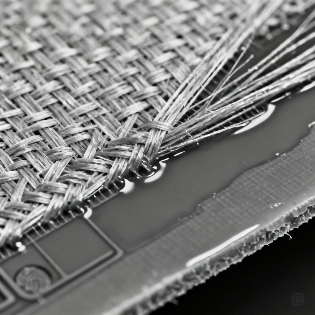
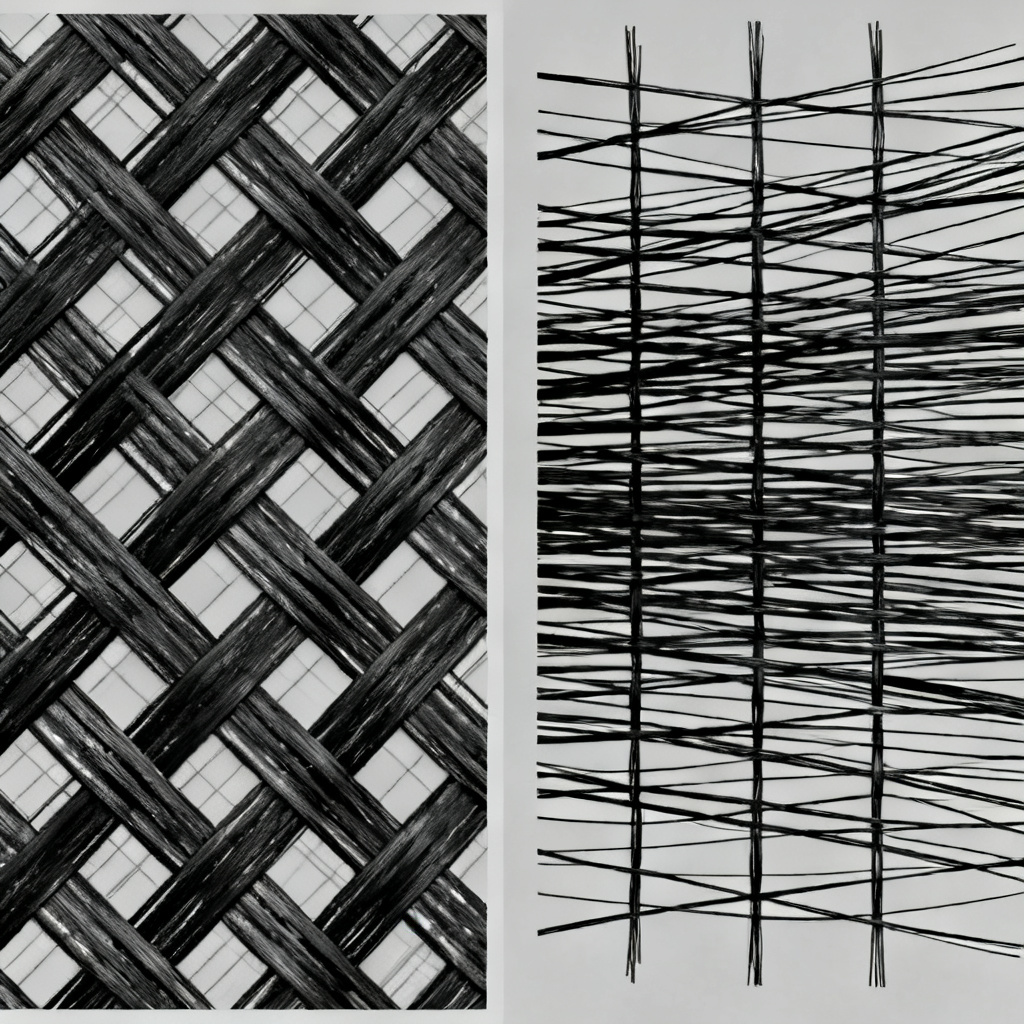
Glass weave is the reinforcing fabric embedded within PCB laminates, typically made from E-glass or S-glass fibers coated with resin. The weave pattern—plain, twill, or satin—determines mechanical and electrical properties. The dielectric constant (Dk) of glass fiber (~6.0–6.5) is significantly higher than resin (~3.0–3.5), creating periodic regions of high and low Dk along a trace. This spatial variation directly impacts differential pair impedance consistency.
Key parameters include fiber diameter (5–9 µm), weave density (thread count), and weave style. Spread-glass weaves (e.g., 1078, 1086) offer more uniform fiber distribution, reducing Dk variation compared to standard plain weaves.
How Glass Weave Effects Cause Impedance Inconsistency in Differential Pairs
When a differential pair is routed over a PCB laminate, traces encounter alternating high Dk (over glass bundles) and low Dk (over resin-rich gaps). This causes characteristic impedance (Z0) to fluctuate. For differential pairs, both odd-mode impedance (Zodd) and coupling between traces are affected, leading to impedance mismatch.
Glass weave effects are frequency-dependent: at high frequencies (>5 GHz), the electric field is more concentrated near the trace, making it sensitive to local Dk variations. Differential pairs are particularly susceptible because phase skew between traces (one over glass, the other over resin) converts common-mode noise into differential-mode noise. For example, a 100-ohm differential pair on standard FR-4 with 2116 weave can experience ±2–5 ohm impedance perturbations per glass bundle, accumulating to 10–20% variation at 10 Gbps.
Quantifying the Impact: Measurement and Simulation
Time-Domain Reflectometry (TDR) Measurements
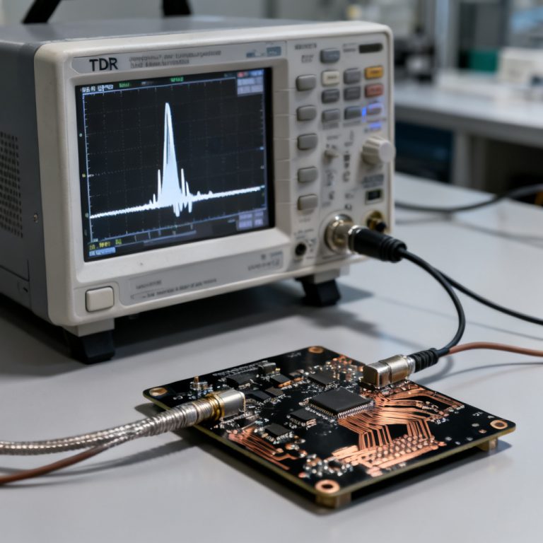
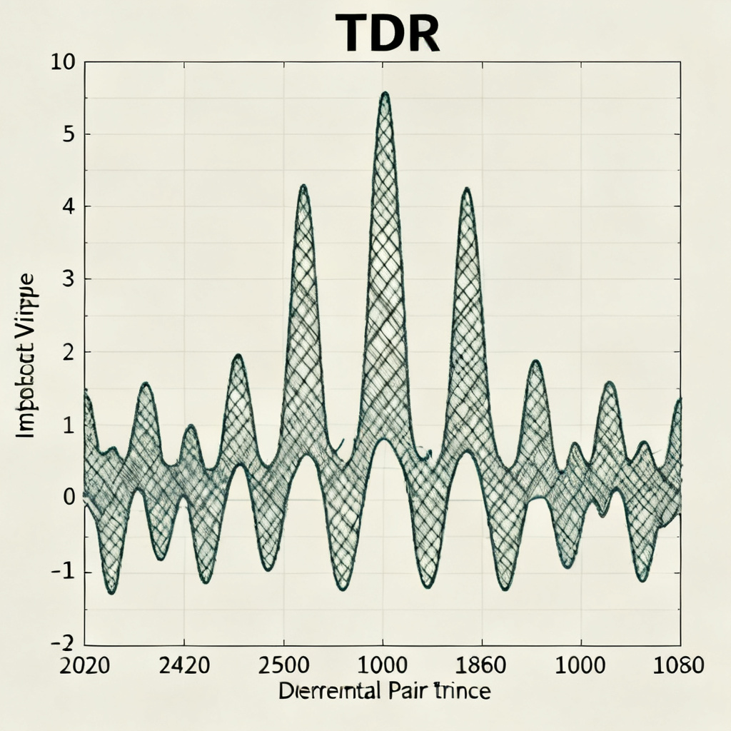
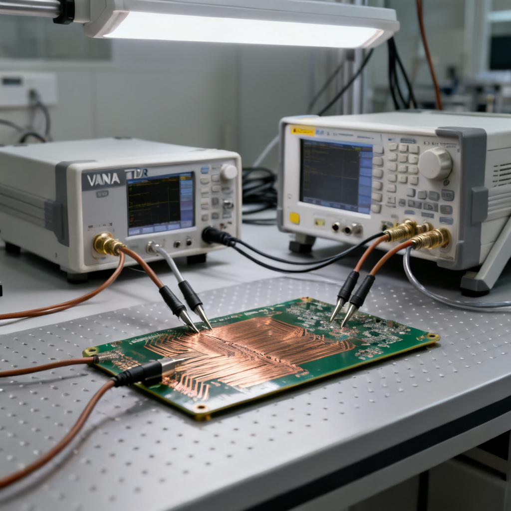
TDR is the primary method to characterize impedance variation. A step pulse is launched into the differential pair, and reflected signals reveal impedance peaks and valleys corresponding to glass bundle and resin gap locations. Peak-to-peak variation typically ranges from 2–8 ohms for standard FR-4, depending on weave style and trace width.
Full-Wave Electromagnetic (EM) Simulation
Tools like Ansys HFSS, CST Microwave Studio, or Keysight ADS model glass weave effects by importing laminate cross-sections with actual fiber distribution. Simulation reveals differential impedance vs. frequency, phase skew between traces, and S-parameter degradation (Sdd21 and Scc21).
Real-World Data from Studies
| Study | Material/Weave | Impedance Variation |
|---|---|---|
| IPC-2141A | 2116 glass, 100 ohm differential pair | 97–103 ohms over 2 cm |
| Isola Group | Spread-glass 1078 | ±1 ohm (vs. ±4 ohm for plain weave) |
| Rogers Corporation | Standard FR-4 at 28 Gbps | 3 dB insertion loss increase due to impedance mismatch |
Mitigation Strategies for Consistent Differential Pair Impedance
Material Selection: Choose Low-Weave-Impact Laminates
Differential pair impedance consistency can be improved by selecting spread-glass weaves (e.g., 1078, 1086, 3313) from suppliers like Isola (I-Speed), Rogers (RO4000 series), or Panasonic (Megtron series). Non-woven laminates (e.g., Rogers RT/duroid) eliminate glass weave entirely, offering near-zero impedance variation but at higher cost. Lower Dk glass fibers (S-glass, Dk ~5.5) also reduce contrast with resin.
Design Techniques: Optimize Trace Routing
Key design techniques include: (1) weave angle routing (5–10 degrees relative to weave direction), which reduces impedance ripple by 50–70%; (2) increasing trace width to average Dk variation over a larger area; (3) using solid ground planes to stabilize the electric field; and (4) matching trace lengths to minimize phase skew.
Manufacturing Considerations
Specify laminate orientation in your PCB stackup to align weave direction with less critical traces. Optimize resin-to-glass ratio with suppliers, and consider post-lamination resin smoothing processes that can reduce Dk variation by up to 40%.
Advanced Techniques for High-Frequency Applications (>25 Gbps)
For data rates above 25 Gbps, use low-loss laminates (e.g., Rogers 4350B, Isola Tachyon) with tighter Dk tolerances. Stripline configurations are less sensitive to glass weave effects than microstrip. Add serpentine delay lines to compensate for phase skew, though this increases design complexity.
Case Studies and Best Practices
Case Study: 25 Gbps Backplane Design
A major networking equipment manufacturer redesigned a backplane for 25 Gbps NRZ signaling. Initial prototypes using standard FR-4 (2116 weave) showed 15% impedance variation, causing bit errors. By switching to spread-glass laminate (Isola I-Speed) and routing differential pairs at 7 degrees to the weave, impedance variation dropped to 3%, and bit error rate improved by 10x.
Best Practices Summary
- Select laminates with spread-glass or non-woven structures for data rates >10 Gbps.
- Use weave angle routing (5–10 degrees) for critical differential pairs.
- Simulate glass weave effects using EM tools before fabrication.
- Require TDR impedance profiles from your PCB manufacturer for quality assurance.
- Consider stackup symmetry and ground plane proximity to stabilize impedance.
Future Trends and Conclusion
Emerging Materials
In support of differential pair routing rules, nanofiber-reinforced laminates (e.g., carbon nanotubes) and adaptive resin systems that compensate for weave effects are under development, promising even better differential pair impedance consistency.
Industry Standards
IPC-2141A provides guidelines for characterizing impedance variation due to glass weave. Future updates may include specific metrics for differential pair consistency.
Conclusion
Glass weave effects are a manageable challenge in high-speed PCB design. By understanding the physics, quantifying impact through simulation and measurement, and applying mitigation strategies, you can achieve consistent differential pair impedance for data rates up to 50 Gbps and beyond. At [Your Company Name], we specialize in manufacturing high-speed PCBs with optimized laminates and precise impedance control. Contact us for a consultation on your next project.
Frequently Asked Questions
What is glass weave effect in PCB?
Glass weave effect refers to the variation in dielectric constant (Dk) along a PCB trace due to the woven glass fiber structure in laminates, which impacts differential pair impedance consistency.
How does glass weave affect differential pair impedance?
The periodic pattern of glass bundles and resin-rich gaps creates local Dk variations, causing impedance fluctuations and phase skew in differential pairs, degrading signal integrity at high speeds.
What materials reduce glass weave effects?
Spread-glass weaves (e.g., 1078, 1086), non-woven laminates (e.g., Rogers RT/duroid), and low-Dk glass fibers (S-glass) minimize glass weave effects and improve impedance consistency.
How can I measure glass weave impact?
Time-domain reflectometry (TDR) and full-wave EM simulation (e.g., Ansys HFSS) are standard methods to quantify impedance variation caused by glass weave structure.
What is weave angle routing?
Weave angle routing involves routing differential pairs at a 5–10 degree angle relative to the weave direction to average Dk variation, reducing impedance ripple by 50–70%.