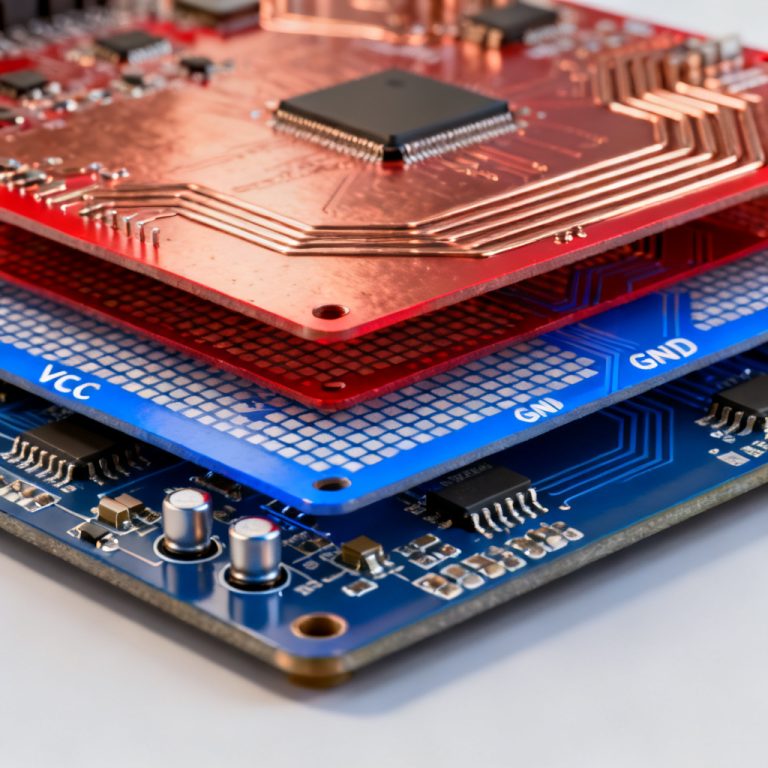
In high-speed PCB design, slots and splits in planes break return path PCB design and signal integrity, causing increased inductance, EMI, and data errors. This comprehensive guide explains the physics, common failure modes, and proven fixes to ensure robust high-speed PCB performance.
Physics of Return Current and Plane Discontinuities in Return Path PCB Design
Why Return Current Stays Close to the Signal (Proximity Effect)
At low frequencies, return current spreads across the entire plane. However, at high frequencies (typically above 1 MHz), the return current is forced by mutual inductance to flow directly beneath the signal trace. This creates a tightly coupled transmission line structure. The return current follows the path of least inductance, which is the path with the smallest loop area. This is why a continuous, unbroken reference plane is non-negotiable for high-speed signals.
What Happens When a Slot or Split is Present
When a signal trace crosses a slot or split in the reference plane, the return current cannot flow directly beneath it. It is forced to go around the edge of the slot. This creates a large current loop. The consequences are:
- Increased Inductance: The detour dramatically increases the loop inductance. For a slot of just 1 cm, the inductance can increase by 10-20 nH, severely degrading signal rise times.
- Common-Mode Conversion: The discontinuity converts differential-mode current into common-mode current, which radiates as EMI and couples into other circuits.
- Voltage Drop and Ground Bounce: The increased impedance causes a voltage drop across the slot, injecting noise into the plane system. This can cause false switching in nearby logic.
- Signal Reflection: The impedance discontinuity (a sudden change in the characteristic impedance) causes reflections, leading to ringing and data errors.
Key Insight: The return current does not “jump” across a slot. It must physically travel around the edge. The farther the detour, the worse the signal integrity.
Common Scenarios Where Slots and Splits Cause Problems in Return Path PCB Design
Crossing a Moat or Split in a Mixed-Signal PCB
Scenario: A digital signal trace crosses from the analog ground plane to the digital ground plane over a moat (a gap between the two planes).
The Problem: The return current must travel all the way to the point where the two planes are connected (e.g., a single bridge or a zero-ohm jumper). This creates a massive loop. The signal may still function, but the radiated EMI will be high, and the analog section will be contaminated with digital noise.
Expert Fix: Never route a signal trace across a split plane unless the return path is provided through a local stitching capacitor or a bridge. The best practice is to:
- Keep all high-speed signals over a single, continuous reference plane.
- If a split is unavoidable, place stitching capacitors (0.1 µF or 1 nF) across the split near the crossing point. This provides a high-frequency AC return path.
- Alternatively, use a bridge (a narrow copper trace connecting the two planes) directly under the signal trace.
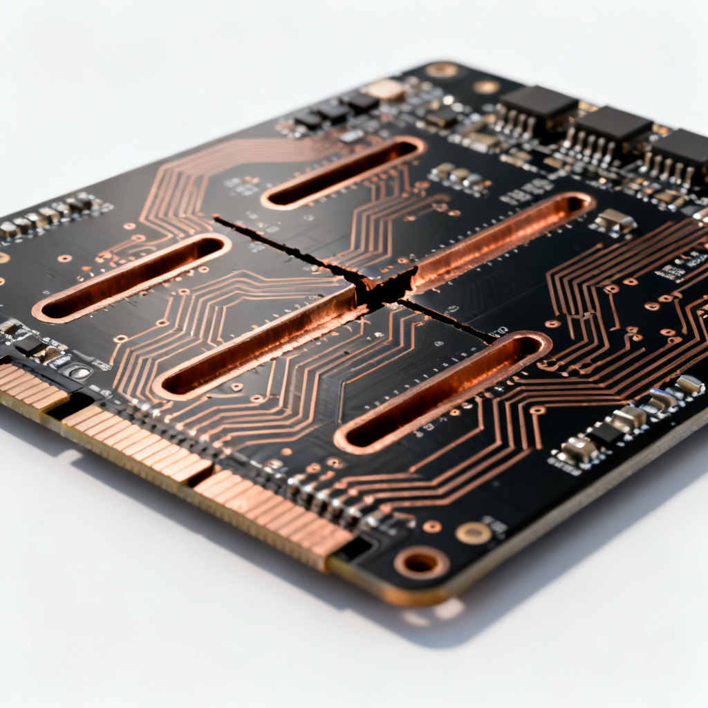
Slots for Connectors (e.g., PCIe, SATA, HDMI)
Scenario: Many high-speed connectors have long slots in the ground plane to accommodate pin fields or isolation requirements. A signal trace (e.g., a differential pair) is routed over this slot.
The Problem: The slot breaks the return path for the signal pair. Even if the pair is differential, the common-mode return current is disrupted. This can cause excessive crosstalk, mode conversion, and failure to meet eye diagram masks.
Expert Fix:
- Use a ground plane under the connector: Ensure that the connector’s ground pins are directly connected to the ground plane with minimal inductance. Add ground vias adjacent to each signal via.
- Avoid routing over the slot: If the slot is unavoidable, use a reference plane on a different layer (e.g., Layer 2) that is continuous under the slot. The signal can reference that layer instead.
- Stitching vias: Place stitching vias along the edges of the slot, connecting the top ground plane to the inner ground plane. This provides an alternative return path for the current flowing around the slot.
Thermal Relief Pads and Isolation Moats
Scenario: A high-speed signal passes near a large thermal relief pad (e.g., for a voltage regulator) that has a moat or cutout in the ground plane around it.
The Problem: The moat creates a discontinuity in the reference plane. Even if the signal does not cross the moat, the return current can be disturbed by the proximity. The fringing fields from the signal trace can couple into the moat, causing noise injection.
Expert Fix:
- Increase clearance: Keep high-speed traces at least 5x the dielectric height away from any plane cutout or moat.
- Use solid plane connections: Where possible, use solid copper connections for thermal relief pads instead of spoke connections. If spokes are required, ensure they are short and wide.
- Ground stitching: Place ground vias around the perimeter of the moat to contain the fields and prevent energy from escaping.
How to Diagnose a Broken Return Path in Return Path PCB Design
Visual Inspection in the Layout Tool
Before fabrication, perform a manual visual check. In your PCB layout software (e.g., Altium, KiCad, Allegro), set the layer stack-up to show the signal layer and the adjacent reference plane simultaneously. Look for:
- Any signal trace that crosses a gap, slot, or cutout in the reference plane.
- Traces that run parallel to a slot edge for more than a few millimeters.
- Vias that are placed without a nearby ground via.
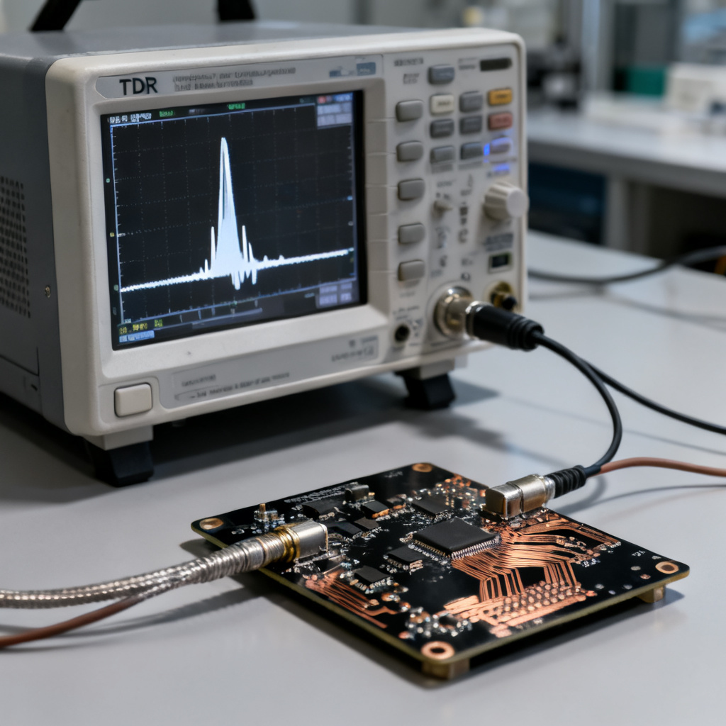
Simulation and Measurement
Use 3D electromagnetic simulation (e.g., Ansys HFSS, CST) to visualize return current density. You can also use a time-domain reflectometer (TDR) on a prototype to measure impedance discontinuities. A TDR will show a spike in impedance at the location of the slot.
Quick Check: If you see excessive crosstalk, EMI, or signal jitter in your design, suspect a broken return path first.
The Definitive Fixes for Return Path PCB Design – A Step-by-Step Guide
Fix 1: Provide a Continuous Reference Plane (The Golden Rule)
The best fix is prevention. Ensure that every high-speed signal has a continuous, unbroken reference plane directly adjacent to it. This means:
- Use a solid ground plane as the primary reference.
- Avoid any splits, moats, or slots under high-speed traces.
- If you must have a split (e.g., for analog/digital separation), place all high-speed signals over one side of the split only.
Fix 2: Stitching Capacitors and Bridges
When a split is unavoidable, use stitching capacitors (for AC coupling) or bridges (for DC coupling).
- Stitching Capacitor: Place a 0.1 µF or 1 nF capacitor (with low ESL) across the split, as close as possible to the signal crossing point. This provides a high-frequency return path.
- Bridge: A narrow copper trace connecting the two plane islands directly under the signal trace. This is ideal for DC-coupled signals.
Important: Use multiple stitching capacitors for multiple signal crossings. One capacitor per crossing is a good rule of thumb.
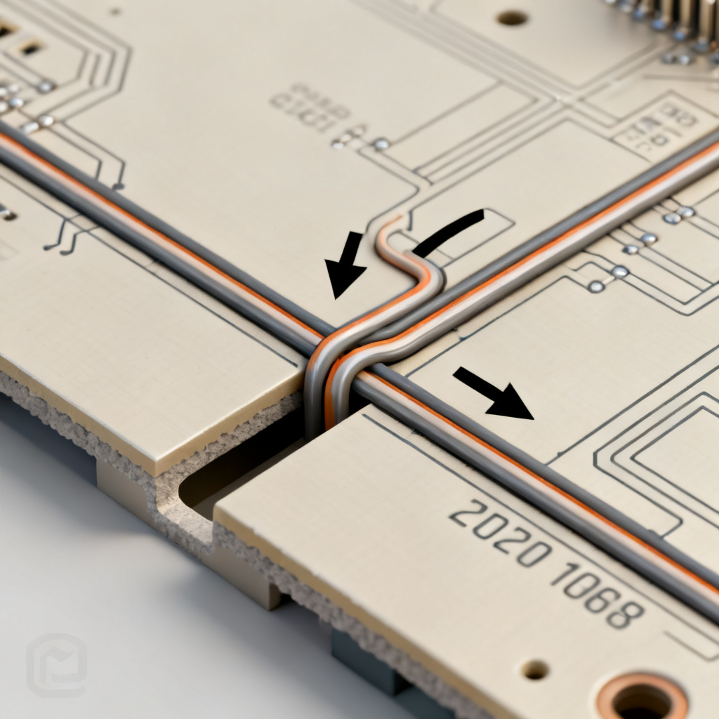
Fix 3: Layer Jumping with Stitching Vias
If you cannot avoid a slot on one layer, move the signal to a different layer where the reference plane is continuous.
- How to do it: Place a via near the slot edge to transition the signal to an inner layer. Then, place a ground stitching via adjacent to the signal via to provide the return current path.
- Rule: For every signal via, place at least one ground via within 1 mm. For differential pairs, place a ground via near each pair.
Fix 4: Use Differential Pair Routing with Care
Differential pairs are often thought to be immune to return path issues because the return current is balanced. However, common-mode return current still needs a path. A slot under a differential pair will cause common-mode noise.
- Fix: Ensure the slot does not run between the two traces. Keep the pair over a continuous plane. If a slot is unavoidable, use a guard trace or ground vias to contain the fields.
Fix 5: Ground Vias at Connectors and Vias
The most common cause of return path failure is inadequate via stitching near connectors.
- Action: Place ground vias every 1-2 mm along the length of a high-speed connector. For each signal via, place a ground via directly adjacent (within 0.5 mm).
- Why: This minimizes the loop area for the return current when it transitions from the PCB to the cable or backplane.

Advanced Considerations in Return Path PCB Design
Slots in Power Planes vs. Ground Planes
While ground planes are the most common reference, power planes are also used. The same rules apply. If a signal references a power plane, any slot or split in that power plane will break the return path. Always ensure the reference plane is continuous.
The Role of Dielectric Thickness
The loop inductance created by a slot is proportional to the distance the return current must travel and inversely proportional to the dielectric thickness. A thinner dielectric (e.g., 4 mils vs. 10 mils) reduces the loop area and inductance. However, it does not eliminate the problem—it only reduces its severity.
When Slots Are Actually Good
Slots are sometimes used intentionally to isolate noisy circuits (e.g., switching regulators) from sensitive analog circuits. In this case, the slot is placed between the circuits, not under the signal traces. Never route a high-speed signal across an isolation slot.
Comparison: Our Return Path PCB Design Expertise vs. Generic PCB Fabricators
| Feature | Our High-Speed PCB Service | Generic PCB Fabricators |
|---|---|---|
| Return Path Analysis | Comprehensive DRC and simulation support | Basic rule checks only |
| Stitching Via Optimization | Custom ground via placement guidance | Standard via patterns |
| Impedance Control | Controlled impedance for 50 Ohm, 100 Ohm | Limited impedance options |
| Stackup Design | Advanced stackup for signal integrity | Standard layer stacks |
Key Terminology for Return Path PCB Design
- Return path: The path that return current takes in a PCB, ideally directly beneath the signal trace.
- Slot: A cutout or gap in a reference plane that interrupts the return path.
- Split plane: A reference plane divided into separate areas, often for analog and digital sections.
- Stitching capacitor: A capacitor placed across a split to provide a high-frequency return path.
- Ground via: A via connecting to the ground plane, used to minimize loop inductance.
- Common-mode noise: Noise that appears equally on both conductors of a differential pair, often caused by return path discontinuities.
FAQ: Return Path PCB Design and Slots in Planes
What is a return path in PCB design?
The return path is the route taken by the return current of a signal. In high-speed PCB design, it must be continuous and directly beneath the signal trace to maintain signal integrity.
How do slots and splits in planes break return path PCB design?
Slots and splits force the return current to detour around the gap, increasing loop inductance and causing signal integrity issues like EMI, crosstalk, and reflections.
How can I fix a broken return path in my PCB?
Use stitching capacitors across splits, add ground vias near signal vias, avoid routing over slots, and ensure a continuous reference plane for all high-speed signals.
What is the difference between a slot and a split in a PCB plane?
A slot is a narrow cutout, often for connectors, while a split is a wide separation between two plane areas, often for isolation. Both disrupt the return path.
Why is return path important for high-speed PCB design?
Without a proper return path, signal integrity degrades due to increased inductance, common-mode noise, and EMI, leading to data errors and system failure.
Conclusion: The Return Path is the Signal Path
In high-speed PCB design, the return path is not an afterthought—it is an integral part of the signal path. Slots and splits in planes are the number one cause of signal integrity and EMI problems that are invisible in schematic review but devastating in prototype testing.
Your Action Checklist:
- Visual check: Ensure no high-speed trace crosses a slot or split.
- Via placement: Always pair signal vias with ground vias.
- Connector design: Stitch ground vias densely around connectors.
- Mixed-signal design: Use a single, continuous ground plane. Do not split it.
- Simulate or measure: Use TDR or EM simulation to verify.
By following these principles, you can ensure your high-speed PCB designs are robust, low-noise, and compliant with signal integrity standards. For custom fabrication of such high-speed PCBs, we offer advanced stack-up support, controlled impedance, and rigorous DRC checks to prevent return path issues before manufacturing.