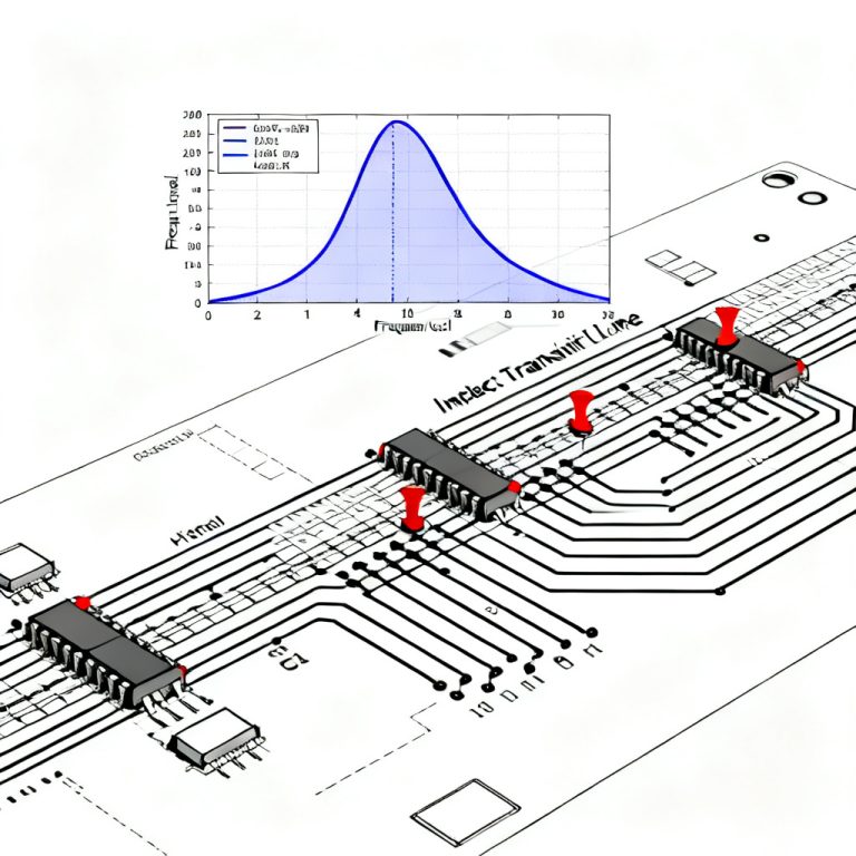
Calibrating your return path PCB design simulation with measured data is essential for high-speed signal integrity. This guide provides a step-by-step process to align simulation models with real-world measurements, ensuring accurate predictions of impedance, crosstalk, and EMI in your high-speed PCB designs.
Why Calibration Matters: The Science of Return Path in High-Speed PCB Design
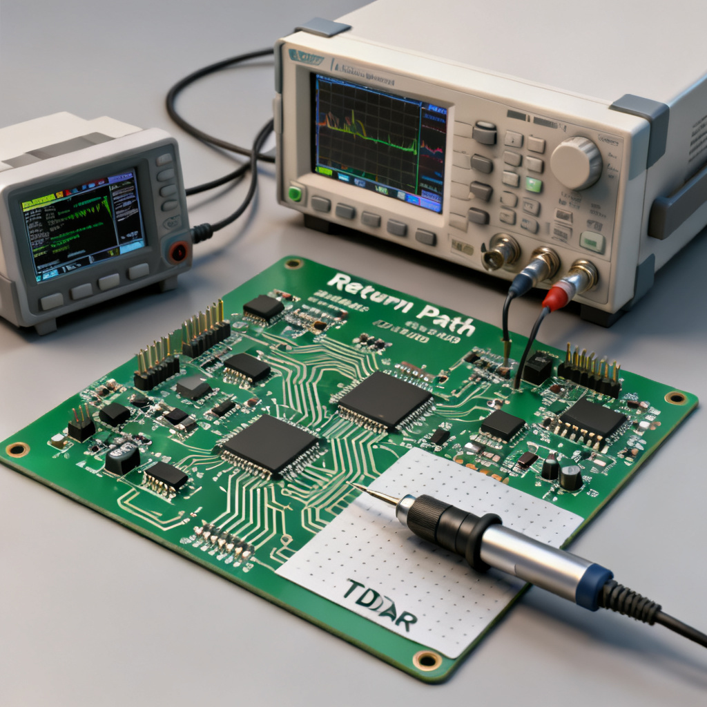
In high-speed PCB design, the return path PCB design simulation must account for every discontinuity. Every signal trace requires a continuous, low-impedance return path directly beneath it, typically on an adjacent ground plane. Discontinuities such as slots in the ground plane, vias, or layer stackup changes disrupt this path, causing current to flow through unintended routes. This leads to increased loop inductance, degraded signal rise times, common-mode noise, EMI, and crosstalk between adjacent traces.
Simulation tools rely on models that may not capture real-world manufacturing tolerances, material properties, or parasitic effects. Calibrating your simulation with measured data ensures your model accurately reflects the physical board, making design decisions reliable for high-speed PCB production.
Step 1: Gather High-Quality Measured Data for Return Path Calibration
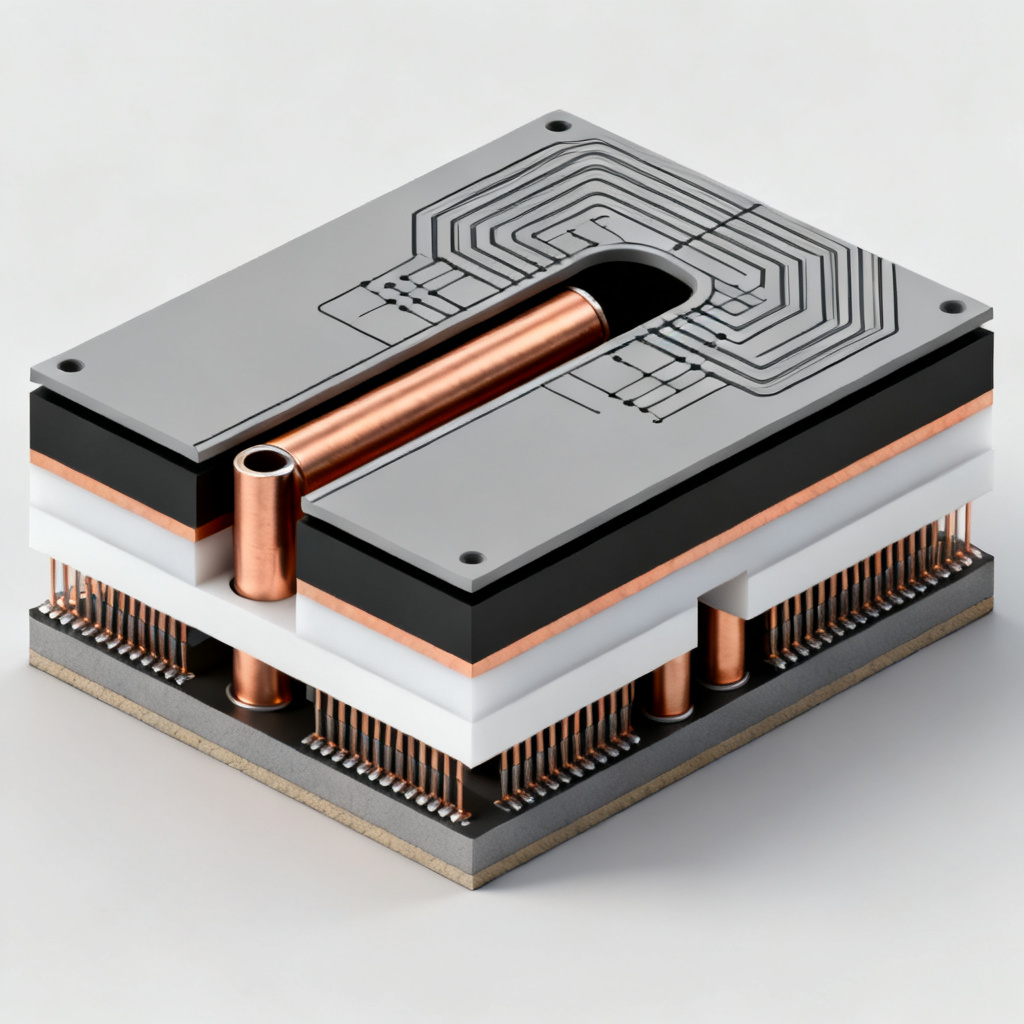
The first and most crucial step in return path PCB design simulation calibration is obtaining accurate measured data from your PCB prototype or test coupon. Without this, calibration is impossible.
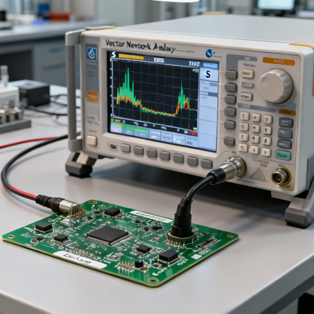
1.1 Use a Vector Network Analyzer (VNA)
For return path PCB design simulation, a VNA is the gold standard for measuring return path characteristics. Calibrate the VNA itself using an SOLT (Short-Open-Load-Thru) or TRL (Thru-Reflect-Line) calibration kit to eliminate systematic errors. Use a 4-port VNA for differential signals to capture mode conversion (S-parameters) that reveal return path issues. Create test coupons replicating critical return path structures, such as microstrip over a ground plane slot or via transitions. Measure S21 (insertion loss) and S11 (return loss) at frequencies up to the 5th harmonic of your signal.
1.2 Extract Time-Domain Reflectometry (TDR) Data
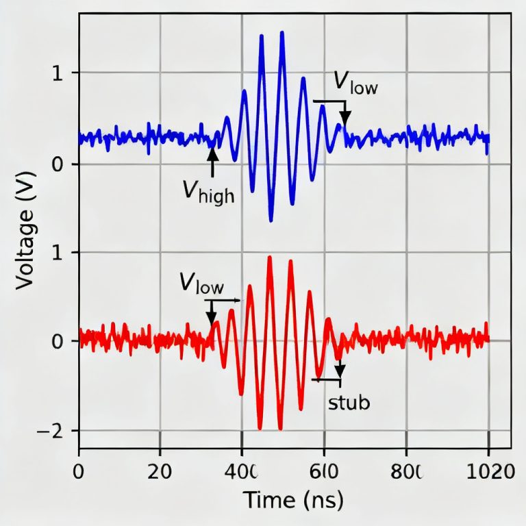
TDR provides a direct view of impedance discontinuities along the return path. A VNA can be converted to TDR via inverse Fourier transform (IFT) using software like MATLAB or Keysight ADS. Use TDR to identify the exact location of return path breaks; a sudden impedance spike at a via transition indicates a poor return path. Measure the impedance profile from driver to receiver and compare with your simulation’s impedance profile to identify discrepancies.
1.3 Capture S-Parameters for Key Structures
For return path PCB design simulation, focus on S-parameters describing the return path loop: S11 (reflection at the driver), S22 (reflection at the load), and S21 (transmission). For differential pairs, measure Sdd21 and Scc21 (common-mode transmission). Use de-embedding techniques like TRL calibration or port extension to remove test fixture and probe effects, ensuring measured data reflects only the PCB structure. Store measured S-parameters as Touchstone (.sNp) files for import into your simulation tool.
Step 2: Build an Accurate Simulation Model for Return Path Analysis
With measured data in hand, create a simulation model that can be calibrated. The model must include all physical details affecting the return path.
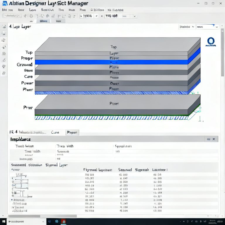
2.1 Define the Geometry and Stackup
Use a 3D full-wave electromagnetic (EM) solver such as Ansys HFSS, Keysight EMPro, or CST Studio for return path PCB design simulation. 2D solvers are insufficient for vias, slots, or non-ideal return paths. Include the exact layer stackup, copper roughness using the Huray or Hammerstad model, and dielectric properties (Dk and Df) from the PCB manufacturer’s datasheet. For high-speed materials like Rogers 4350B or Megtron 6, use measured Dk at the operating frequency. Model the return path as a loop, including ground plane, slots, via barrels, antipads, and reference plane transitions.
2.2 Set Up Ports and Excitations
Use wave ports or lumped ports with a reference impedance of 50 ohms (single-ended) or 100 ohms (differential). For return path PCB design simulation, add ports at the driver and load, defining the return path as the ground reference. For differential pairs, use differential ports. Ensure port geometry matches the physical launch, such as microstrip, stripline, or coplanar waveguide.
2.3 Simulate the Baseline Model
Run the simulation and export S-parameters. Compare simulated S11 and S21 with measured data. Note differences in resonance frequencies, impedance dips, and insertion loss slopes. Use the TDR impedance profile from the simulation via IFT of S11 to identify where the model deviates from measurement. Common discrepancies include dielectric constant (Dk) mismatch, copper roughness, and via stub resonance. Document the baseline error, such as ±5% impedance variation or ±0.5 dB insertion loss error, to set calibration targets.
Step 3: Perform Calibration Using Measured Data for Return Path Models
Calibration is an iterative process where you adjust simulation parameters until the model matches measured data within an acceptable tolerance.
3.1 Adjust Material Properties
The most common calibration step is to tune Dk and loss tangent (Df) of the substrate. Use measured S-parameters to extract effective Dk via the phase delay method from the phase of S21. If measured resonance frequency is lower than simulated, decrease Dk by 0.2–0.5. Copper roughness is often underestimated; use the Huray model with a roughness factor of 1.0–2.0 µm for standard copper and adjust until insertion loss slope matches measured data. Dielectric thickness can vary by ±10% due to manufacturing tolerances; adjust substrate height in simulation to match measured impedance.
3.2 Tune Geometry and Parasitics
For via transitions, adjust antipad diameter, via barrel diameter, and number of stitching vias. Increasing antipad clearance reduces parasitic capacitance and shifts resonance frequency. For return path slots, measure slot dimensions using a microscope or X-ray and adjust slot width in simulation by ±0.1 mm to match measured TDR impedance spike. For differential pairs, adjust trace spacing and width to match measured differential impedance using Sdd11 and Sdd21.
3.3 Use Optimization Algorithms
Most EM solvers have built-in optimization tools. Define an error function such as mean squared error between simulated and measured S-parameters, and let the solver automatically adjust parameters like Dk, Df, trace width, and via dimensions within a defined range. Use a gradient-based optimizer for linear parameters and a genetic algorithm for non-linear parameters. Set a tolerance of 1% for impedance and 0.1 dB for insertion loss. Perform sensitivity analysis first to identify which parameters most affect the return path, then optimize high-sensitivity parameters first.
3.4 Validate with Time-Domain and Frequency-Domain Metrics
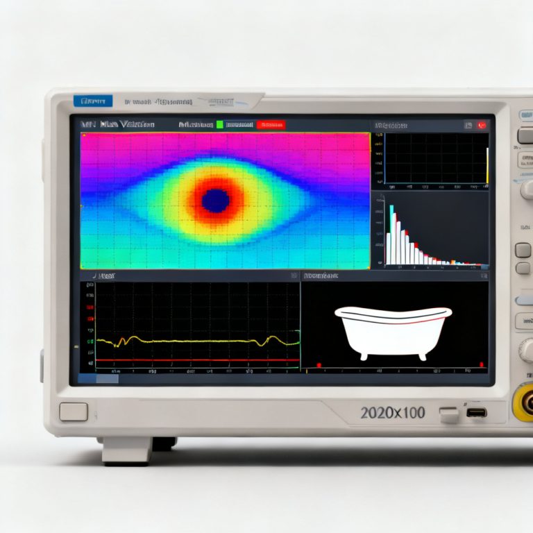
After calibration, compare simulated TDR impedance profile with measured profile; they should match within 2–3 ohms across the entire trace. Check S21 phase response for linearity, indicating no major reflections. Use the calibrated model to predict the eye diagram via channel simulation; the model should predict eye height within 5% and jitter within 2 ps. Perform cross-validation by simulating a different structure, such as a different via transition or longer trace, and compare with its measured data. Consistent error indicates robust calibration.
Step 4: Apply the Calibrated Return Path Model to Your High-Speed PCB Design
Once the return path PCB design simulation is calibrated, use it confidently to optimize your high-speed PCB design. The calibrated model accounts for real-world effects, enabling accurate what-if analyses.
4.1 Optimize Return Path Continuity
Use the calibrated model to test different return path strategies: adding stitching vias, widening ground plane slots, or using embedded microstrip. If the calibrated model shows a 3 dB loss peak at 8 GHz due to a via stub, add back-drilling to remove the stub. Simulate the impact of return path discontinuities on crosstalk and adjust trace spacing or add guard traces. Validate the final design with the calibrated model before fabrication to reduce EMI or signal integrity failures.
4.2 Create a Design of Experiments (DoE)
Use the calibrated model to run a DoE varying manufacturing tolerances, such as ±10% stackup thickness and ±5% Dk. Identify the worst-case return path impedance and ensure it stays within specification, for example 50 ohms ±10%. For high-volume production, define acceptable limits for S-parameters like S11 < -15 dB up to 10 GHz, making this part of your DFM checklist. Document the calibration process and final model parameters, such as Dk = 3.8, Df = 0.005, copper roughness = 1.5 µm, as a reference for future designs using the same material and stackup.
4.3 Automate the Calibration Workflow
For recurring projects, create a script in Python or MATLAB that automates comparison of simulated and measured S-parameters and adjusts model parameters, reducing manual effort and ensuring consistency. Integrate the calibration process into your design tool using APIs, automatically comparing simulated TDR with measured TDR from a test coupon. Share the calibrated model with your PCB manufacturer so they can optimize fabrication processes, such as adjusting etch compensation, to match the model.
Common Pitfalls in Return Path PCB Design Simulation Calibration
Even with a robust calibration process, engineers encounter challenges. Here are common pitfalls and how to avoid them.
Pitfall 1: Ignoring High-Frequency Effects
Many engineers calibrate only at low frequencies like 1 GHz but ignore higher harmonics, leading to inaccurate predictions for fast rise times. Always calibrate up to the 5th harmonic, for example 10 GHz for a 2 Gbps signal. Skin effect and dielectric relaxation are frequency-dependent; use a frequency-dependent Dk and Df model like Djordjevic-Sarkar for accuracy above 10 GHz.
Pitfall 2: Overfitting the Model
Adjusting too many parameters, such as 10+ variables, can lead to a model that matches measured data but fails for other structures. Stick to 3–5 key parameters like Dk, Df, trace width, and via antipad, and validate with cross-validation.
Pitfall 3: Neglecting the Test Fixture
VNA cables, connectors, and probes add their own parasitics. Always use de-embedding like TRL calibration to remove their effects; otherwise, you calibrate to the fixture, not the PCB. For differential measurements, ensure the test fixture has a balanced return path to avoid common-mode noise corrupting data.
Pitfall 4: Assuming a Perfect Ground Plane
Real PCBs have slots, cutouts, and via antipads that disrupt the return path. Always model the ground plane as a 3D structure, not an ideal solid plane. Use measured TDR to identify hidden discontinuities.
FAQ: Return Path PCB Design Simulation Calibration
What is the importance of return path in high-speed PCB design?
The return path is critical for signal integrity; a poorly calibrated return path PCB design simulation can lead to inaccurate predictions of crosstalk, impedance mismatches, and EMI.
How do I calibrate my return path simulation using a VNA?
Use a VNA with SOLT or TRL calibration, measure S-parameters for key structures, and compare with your return path PCB design simulation to adjust material properties and geometry.
What are common errors in return path simulation calibration?
Common errors include ignoring high-frequency effects, overfitting the model, neglecting test fixture parasitics, and assuming a perfect ground plane.
Can I automate the calibration process?
Yes, create scripts in Python or MATLAB to automate comparison and adjustment, integrating with tools like Altium or Cadence for consistent return path PCB design simulation.
Comparison Table: Calibration Methods for Return Path PCB Design Simulation
| Method | Key Parameters | Advantages | Limitations |
|---|---|---|---|
| VNA-based S-parameter calibration | Dk, Df, trace width, via geometry | High accuracy up to millimeter-wave frequencies | Requires expensive equipment and de-embedding |
| TDR impedance profile calibration | Impedance discontinuities, via stubs | Direct visualization of return path issues | Lower frequency resolution compared to VNA |
| Optimization algorithm calibration | Multiple variables (Dk, Df, copper roughness) | Automated, reduces manual iteration | Risk of overfitting without cross-validation |
Glossary of Key Terms for Return Path PCB Design Simulation
- Return path: The continuous low-impedance path for signal current to return to its source, typically through a ground plane.
- Signal integrity (SI): The quality of an electrical signal in terms of timing, voltage levels, and noise immunity.
- Vector Network Analyzer (VNA): A device that measures S-parameters of high-frequency networks.
- Time-Domain Reflectometry (TDR): A technique to measure impedance variations along a transmission line.
- De-embedding: Removing the effects of test fixtures and probes from measurement data.
- Copper roughness: Surface texture of copper traces that increases high-frequency loss.
- Via stub: The unused portion of a via that causes resonance and signal degradation.