Learn how to generate impedance control PCB reports for your fabricator with precision. This guide covers stackup design, test coupons, and TDR verification to ensure first-pass success for your high-speed designs.

In the world of high-speed PCB design, impedance control is non-negotiable. Whether you are designing for RF, DDR memory, or high-speed serial interfaces (like PCIe, USB 3.0, or HDMI), a mismatch in characteristic impedance can lead to signal reflections, data errors, and complete board failure.
Your PCB fabricator is not a mind reader. To produce boards that meet your exact impedance targets—typically 50Ω single-ended or 100Ω differential—they need a clear, standardized impedance control PCB report. This document bridges the gap between your design intent and the manufacturing reality.
This guide compiles the best practices from industry leaders to teach you exactly how to generate a report that fabricators trust. We will cover:
- The critical information your fabricator needs from you.
- How to design the correct stackup and target impedances.
- The role of test coupons and TDR (Time Domain Reflectometry).
- Common pitfalls and how to avoid them.
By the end of this page, you will be able to create a report that minimizes back-and-forth communication, reduces prototype spins, and guarantees your high-speed PCBs perform as designed.
1. The Foundation – Understanding What Your Fabricator Needs for Impedance Control PCB Reports
Before you open your EDA tool, you must understand what your fabricator requires. The goal of the impedance control PCB report is to give the manufacturer a clear, unambiguous target. Based on industry standards and fabricator feedback, your report must include the following core elements:
1.1. The Target Impedance and Tolerance
This is the most basic requirement. You must specify the exact impedance value for every net or net class.
- Single-ended: Typically 50Ω, but can be 40Ω, 60Ω, or 75Ω for specific applications.
- Differential: Typically 90Ω (USB, PCIe), 100Ω (LVDS, Ethernet), or 85Ω (DDR4/DDR5).
- Tolerance: Industry standard is ±10%. For very high-speed designs (e.g., 25Gbps+), you may request ±5% or even ±3%. Important: Tighter tolerances increase cost. Only specify them where absolutely necessary.
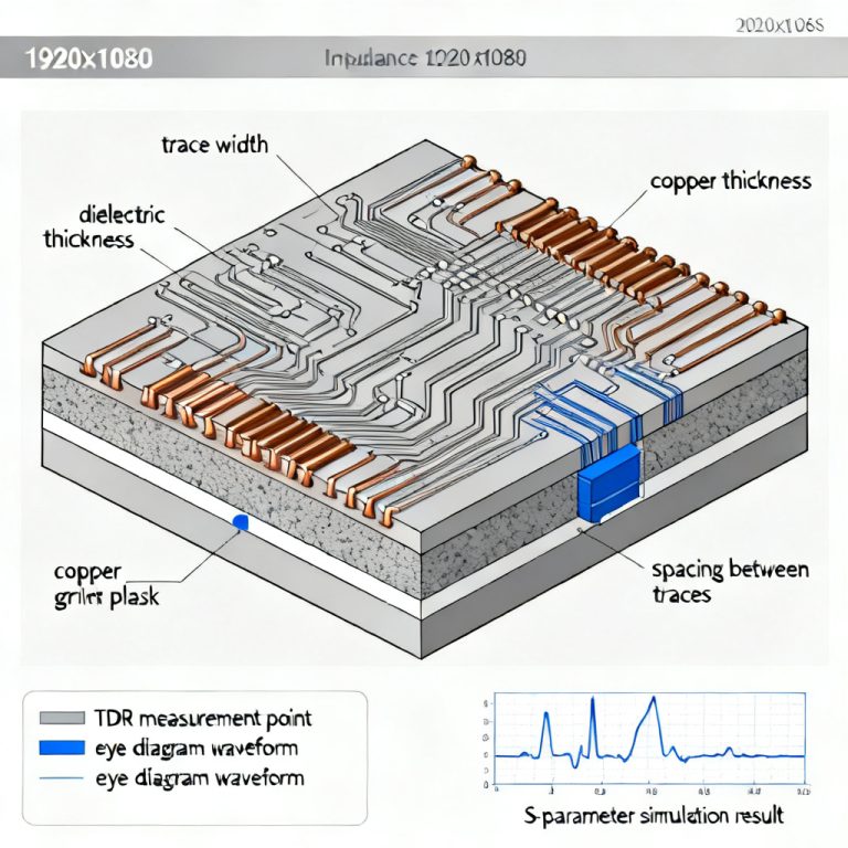
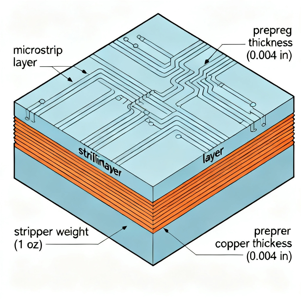
1.2. The Controlled Impedance Layer Stackup
You do not need to provide the final, exact stackup from the fabricator. Instead, provide a target stackup that shows:
- The number of layers.
- The target thickness of each layer (core and prepreg).
- The copper weight (e.g., 0.5oz, 1oz, 2oz).
- The material type (e.g., FR4, Isola 370HR, Rogers 4350B, Megtron 6).
- Which layers are designated for impedance control (signal layers) and which are reference planes (ground/power layers).
1.3. The Material Specification
Impedance is heavily dependent on the dielectric constant (Dk) and dissipation factor (Df) of the laminate. You must specify:
- Material Grade: Standard FR4 vs. high-speed/low-loss materials.
- Dk Value: Use the manufacturer’s datasheet value. Be aware that Dk changes with frequency (e.g., Dk at 1GHz vs. 10GHz).
- Weave Style: For high-speed, specify a low-profile or spread-glass weave (e.g., 1067, 1078, 1080, 2116, 3313) to avoid glass-weave skew.
1.4. Trace Geometry and Reference Planes
Your impedance control PCB report must clearly state:
- Target Trace Width: The width on the inner layer (after etching).
- Target Trace Spacing: For differential pairs (edge-to-edge).
- Reference Planes: Every impedance trace must be directly adjacent to a solid reference plane (ground or power). Specify the plane layers (e.g., L2, L4). Never route impedance traces over a split plane or a void.
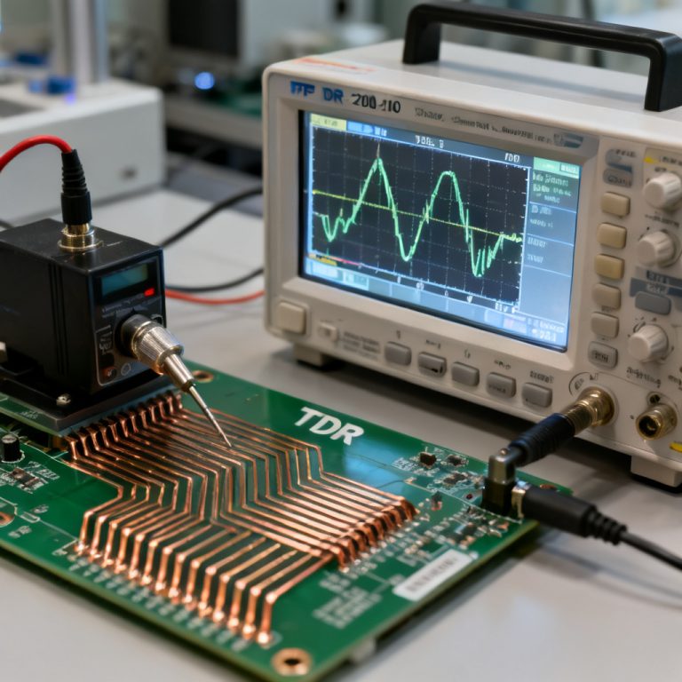
1.5. Test Coupon Requirements
Fabricators use test coupons to physically measure impedance. Your report should specify:
- Coupon Location: Typically on the production panel (scrap area) or on the PCB edge.
- Coupon Design: The coupon must replicate the exact stackup, trace width, and spacing of the actual board. The trace length should be long enough for a TDR probe (usually > 3 inches).
- Number of Coupons: At least one per impedance type per layer. For complex boards, one per net class.
1.6. The Final Report Format
Most fabricators accept reports in PDF or Excel format, but a structured table is preferred. A good report includes:
- A header with project name, date, and contact.
- A stackup diagram.
- A table listing every impedance-controlled net and its target value.
- A section for test coupon specifications.
2. Designing the Stackup and Calculating Target Impedances for Impedance Control PCB Reports
This is the most technical step. You must translate your electrical requirements into physical dimensions. While your fabricator will perform the final calculation, providing a starting point shows you understand the process.
2.1. The Core Equation (Simplified)
For a microstrip (top/bottom layer) and stripline (inner layer), impedance is primarily a function of:
- H: Height of the dielectric above the reference plane.
- W: Trace width.
- T: Copper thickness.
- Er: Dielectric constant.
Microstrip (Surface Layer):
- Impedance is sensitive to the solder mask. Solder mask reduces impedance by 2-4Ω. You must account for this.
- Use the formula:
Z0 = (87 / sqrt(Er + 1.41)) * ln(5.98 * H / (0.8 * W + T))
Stripline (Inner Layer):
- More predictable because it is surrounded by dielectric.
- Use the formula:
Z0 = (60 / sqrt(Er)) * ln(4 * H / (0.67 * π * (0.8 * W + T)))
2.2. Using a Field Solver (The Professional Way)
Manual formulas are approximations. For production-level accuracy, use a 2D field solver like:
- Polar Instruments Si9000: The industry standard. It accounts for surface roughness, solder mask, and specific material Dk.
- Altium Designer / Cadence Allegro: Built-in impedance calculators.
- Saturn PCB Toolkit: A free, reliable tool.
How to use the solver:
- Select the correct topology (Microstrip, Stripline, Asymmetric Stripline).
- Input the dielectric material and its Dk at your operating frequency.
- Input the target impedance (e.g., 50Ω).
- Input the copper weight and dielectric height.
- The solver will output the required trace width (W) and spacing (S).
2.3. The Stackup Table Example
| Layer | Type | Material | Thickness (mils) | Copper Weight (oz) | Target Impedance | Trace Width | Spacing |
|---|---|---|---|---|---|---|---|
| L1 | Signal (Microstrip) | Prepreg 1080 | 3.5 | 1 | 50Ω | 8.5 | N/A |
| L2 | Ground Plane | Core | 5.0 | 1 | N/A | N/A | N/A |
| L3 | Signal (Stripline) | Prepreg 2116 | 4.5 | 0.5 | 100Ω Diff | 5.0 | 8.0 |
| L4 | Power Plane | Core | 5.0 | 1 | N/A | N/A | N/A |
Important: The thickness values (H) are after lamination. Your fabricator will adjust these based on their exact materials and press cycles. Your job is to provide the target.
3. The Art of Test Coupon Design for Impedance Control PCB Reports
Your impedance control PCB report is useless without a plan for verification. The test coupon is the physical witness line that the fabricator measures.
3.1. Coupon Types
- IPC Coupons: Standardized coupons per IPC-2141 or IPC-2221. They include specific patterns for impedance, crosstalk, and propagation delay.
- Custom Coupons: For unique stackups or geometries.
- Edge Coupons: Small, simple coupons placed on the PCB edge. They are cheap but less accurate because they do not represent the internal board environment perfectly.
- Panel Coupons: Larger coupons placed in the scrap area of the production panel. These are more accurate and are the standard for high-volume production.
3.2. What the Coupon Must Include
- Trace Length: Minimum 3 inches (75mm) for accurate TDR measurement.
- Launch Pads: Large pads (e.g., 50×50 mils) at both ends for the TDR probe.
- Ground Connection: A nearby via or solid copper area for the probe ground. The ground and signal launch pads should be clearly labeled.
- Replication: The coupon must have the exact same stackup, copper thickness, and dielectric height as the actual board. Do not change the prepreg or core in the coupon area.
3.3. Example Coupon Specification in Your Report
Coupon ID: C1
Impedance Target: 50Ω Single-ended
Layer: L1 (Microstrip)
Trace Width: 8.5 mils
Trace Length: 4 inches
Reference Plane: L2 (Ground)
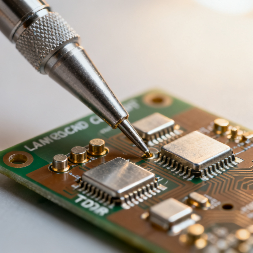
Test Method: TDR (Time Domain Reflectometry) with 35ps rise time.
Acceptance Criteria: 50Ω ± 5Ω (10% tolerance).
4. Common Mistakes and How to Avoid Them in Impedance Control PCB Reports
Even experienced engineers make these errors. Avoid them to save time and money.
4.1. Providing Incomplete Information
- Mistake: Only saying “50Ω impedance” without specifying which layers or nets.
- Solution: Create a net class table in your report. List every net (e.g.,
USB_DP,USB_DN,CLK_P,CLK_N) and its target value.
4.2. Ignoring the Solder Mask Effect
- Mistake: Designing microstrip traces for 50Ω without considering that the solder mask will lower the impedance by 2-4Ω.
- Solution: In your field solver, include a solder mask layer with a thickness of 0.5–1.0 mils and a Dk of 3.5–4.0. Adjust your trace width accordingly.
4.3. Routing Over Split Planes
- Mistake: Routing a 50Ω trace over a gap in the ground plane. This destroys the return current path and causes impedance discontinuity.
- Solution: Ensure every impedance trace has a continuous, solid reference plane directly below (or above) it. If you must cross a split, use stitching capacitors or route on a different layer.
4.4. Using the Wrong Material Dk
- Mistake: Using the Dk value from a generic FR4 datasheet (e.g., 4.5) when your actual material (e.g., Isola 370HR) has a Dk of 4.1.
- Solution: Always use the Dk value provided by your specific laminate manufacturer at your operating frequency. Include this specification in your report.
4.5. Forgetting to Specify the Test Coupon Location
- Mistake: Not telling the fabricator where to place the coupon.
- Solution: Add a mechanical drawing or note in your report: “Place impedance test coupons on the top and bottom of the production panel, adjacent to the board array.”
4.6. Not Accounting for Etch Factor
- Mistake: Designing traces assuming a perfectly rectangular cross-section. In reality, etching creates a trapezoidal shape (wider at the base, narrower at the top).
- Solution: Specify the “target width after etch” or “final width.” Most fabricators can provide their etch factor. A typical assumption is that the top width is 0.5–1.0 mils narrower than the bottom width.
5. The Complete Impedance Control PCB Report Template
Below is a structured template you can copy into your report. Use this as the final deliverable to your fabricator.
5.1. Report Header
- Project Name: [e.g., High-Speed ADC Board v2.1]
- Date: [YYYY-MM-DD]
- Designer: [Your Name / Company]
- Contact Email: [your@email.com]
- Target Fabricator: [Optional, but helpful]
5.2. Stackup Summary Table
(Include a diagram of the layer stackup here. The table below is the data.)
| Layer | Type | Material | Core/Prepreg | Thickness (mils) | Copper Weight (oz) | Notes |
|---|---|---|---|---|---|---|
| Top | Signal | Prepreg 1080 | Prepreg | 3.5 | 1 | Microstrip, solder mask included |
| L2 | Ground | Core | Core | 5.0 | 1 | Solid plane |
| L3 | Signal | Prepreg 2116 | Prepreg | 4.5 | 0.5 | Stripline |
| L4 | Power | Core | Core | 5.0 | 1 | Solid plane |
| Bottom | Signal | Prepreg 1080 | Prepreg | 3.5 | 1 | Microstrip, solder mask included |
5.3. Impedance Net Table
| Net Name | Layer | Topology | Target Impedance | Tolerance | Trace Width (mils) | Spacing (mils) | Reference Plane |
|---|---|---|---|---|---|---|---|
CLK_P | L1 | Microstrip | 50Ω | ±10% | 8.5 | N/A | L2 |
CLK_N | L1 | Microstrip | 50Ω | ±10% | 8.5 | N/A | L2 |
USB_DP | L3 | Stripline | 90Ω Diff | ±10% | 5.0 | 8.0 | L2 & L4 |
USB_DN | L3 | Stripline | 90Ω Diff | ±10% | 5.0 | 8.0 | L2 & L4 |
ETH_P | Bottom | Microstrip | 100Ω Diff | ±10% | 7.0 | 10.0 | L4 |
ETH_N | Bottom | Microstrip | 100Ω Diff | ±10% | 7.0 | 10.0 | L4 |
5.4. Test Coupon Specification
| Coupon ID | Layer | Topology | Target Impedance | Trace Width | Spacing | Length | Reference Plane | Location |
|---|---|---|---|---|---|---|---|---|
| C1 | L1 | Microstrip | 50Ω SE | 8.5 | N/A | 4.0 in | L2 | Panel scrap, top edge |
| C2 | L3 | Stripline | 90Ω Diff | 5.0 | 8.0 | 4.0 in | L2 & L4 | Panel scrap, bottom edge |
| C3 | Bottom | Microstrip | 100Ω Diff | 7.0 | 10.0 | 4.0 in | L4 | Panel scrap, bottom edge |
5.5. Material and Manufacturing Notes
- Laminate: [e.g., Isola 370HR, Dk = 4.1 @ 1GHz]
- Prepreg Weave: [e.g., 1080, low-profile glass]
- Solder Mask: [e.g., LPI Green, thickness 0.5 mils]
- Copper Foil: [e.g., Reverse-treated foil for better adhesion]
- TDR Rise Time: [e.g., 35ps or faster]
- Acceptance Criteria: Impedance values must fall within the specified tolerance for all coupons. Any out-of-spec coupon will require a root cause analysis.
FAQ: Impedance Control PCB Reports for Your Fabricator
What is an impedance control PCB report?
An impedance control PCB report is a document that communicates your design’s target impedance values, stackup, and test coupon requirements to your fabricator, ensuring accurate manufacturing.
Why do I need an impedance control PCB report for high-speed designs?
For high-speed designs, signal integrity depends on consistent impedance. A report helps your fabricator match your specifications, reducing signal reflections and data errors.
How do I create an impedance control PCB report?
Start by defining target impedances for each net, design a stackup with material specifications, and include test coupon details. Use the template in this guide for a complete report.
What information must an impedance control PCB report include?
Your report must include target impedance and tolerance, controlled impedance layer stackup, material specification, trace geometry, reference planes, and test coupon requirements.
How does a fabricator use an impedance control PCB report?
The fabricator uses the report to set up their manufacturing process, adjust etch parameters, and measure test coupons with TDR to verify that the final board meets your impedance targets.
Conclusion: The Path to First-Pass Success with Impedance Control PCB Reports
Generating a proper impedance control PCB report is not just about filling out a form. It is about communicating your design intent with clarity and precision. By providing a complete report that includes a target stackup, net-specific targets, and clear test coupon requirements, you enable your fabricator to:
- Optimize their process to hit your targets.
- Verify the results quickly and accurately.
- Avoid costly re-spins due to impedance mismatches.
Remember, your fabricator is your partner. A well-written report saves both of you time, money, and frustration. Use the template and principles in this guide, and you will consistently get high-quality, high-speed PCBs that perform exactly as you designed.
Ready to produce your next high-speed PCB? Use the checklist below to ensure your report is complete.
Impedance Report Checklist:
- [ ] Net list with target impedances and tolerances.
- [ ] Layer stackup with material type and thickness.
- [ ] Trace width and spacing for each net class.
- [ ] Reference plane layers identified.
- [ ] Solder mask effect accounted for.
- [ ] Test coupon design and location specified.
- [ ] Material Dk and weave style specified.
- [ ] TDR rise time and acceptance criteria stated.

“`