When return path PCB design forces current through a capacitor, it creates impedance discontinuities, increases EMI, and degrades signal integrity in high-speed PCB systems. This comprehensive guide explains the physics, consequences, and mitigation strategies for this critical high-speed PCB design challenge.
Physics of Return Path PCB Design Forces Current Through a Capacitor
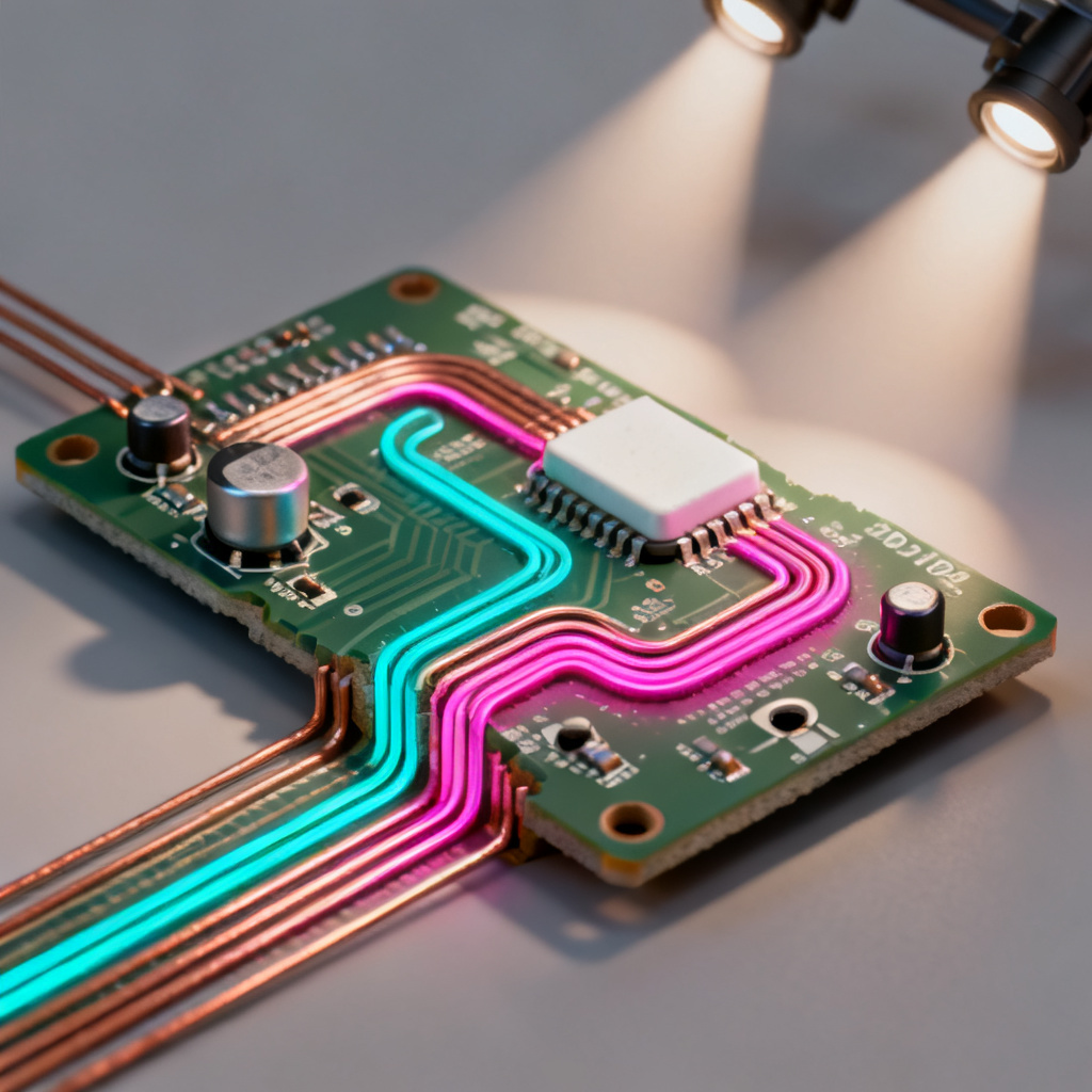
In high-speed PCB design, signal integrity depends critically on the return path. When a high-speed signal propagates along a trace, the electromagnetic field couples the signal current with a return current flowing in the adjacent reference plane. This return current naturally follows the path of least impedance, not least resistance. For high frequencies, this path is the one with the lowest loop inductance.
The Problem of Layer Transition
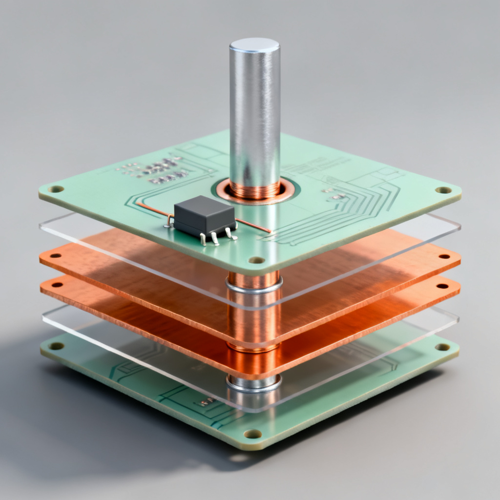
When a signal trace changes layers, the return current must also change its reference plane. If the new reference plane is a different net, the return current cannot simply jump. It must find a path back to the original plane. The most common solution is using a stitching capacitor or decoupling capacitor placed near the via. However, return path PCB design forces current through a capacitor introduces several immediate problems.
What Happens When Current is Forced Through a Capacitor
The capacitor is not an ideal component at high frequencies. It has parasitic elements: Equivalent Series Inductance (ESL), Equivalent Series Resistance (ESR), and self-resonant frequency. Forcing return current through this non-ideal device creates:
- Impedance Discontinuity: The capacitor introduces a high-impedance path at the frequency of interest. This impedance mismatch causes signal reflections, ringing, and increased insertion loss.
- Increased Loop Area: Instead of the return current flowing directly under the signal trace, it must travel from the via, through the capacitor’s pads, and back to the original plane. This creates a large current loop that acts as an efficient antenna for EMI.
- Common-Mode Current Generation: The impedance discontinuity can convert a clean differential signal into common-mode current, causing radiated emissions that fail FCC/CE compliance.
Three Critical Consequences of Return Path PCB Design Forces Current Through a Capacitor
Consequence 1: Signal Quality Degradation
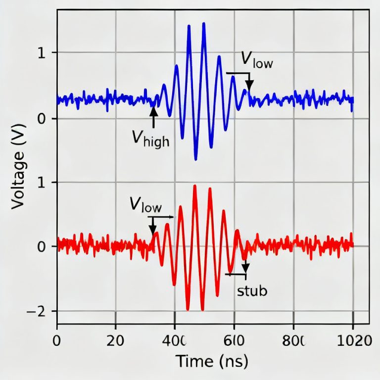
When return path PCB design forces current through a capacitor, the inductance of the capacitor (ESL) is the primary culprit. A typical 0402 capacitor has an ESL of ~500 pH. At 1 GHz, this creates an impedance of ~3.14 Ohms—a massive discontinuity compared to the ~50 Ohm trace impedance. The signal experiences a voltage drop across the capacitor, manifesting as a negative reflection in the signal waveform. The reflected energy travels back to the driver, causing ringing and overshoot.
- Rise Time Blurring: The inductive path slows the return current’s ability to respond to the signal’s fast edge, effectively increasing the rise time and reducing timing margin for high-speed interfaces like DDR, PCIe, or Gigabit Ethernet.
- Ground Bounce: If multiple signals transition across the same capacitor, the cumulative return current creates a voltage spike across the capacitor’s inductance, corrupting other logic gates sharing the same reference plane.
Consequence 2: Increased Electromagnetic Interference (EMI)
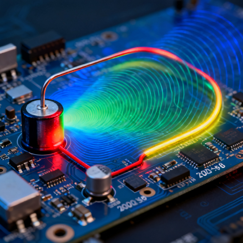
The loop formed by the signal trace, the via, the capacitor, and the return plane is the primary antenna for common-mode radiation. This current loop acts as a magnetic dipole antenna, with radiation efficiency proportional to its area and the square of the frequency. Return path PCB design forces current through a capacitor creates differential-to-common mode conversion, where magnetic fields from the signal and return current no longer cancel out. The common-mode current propagates along attached cables, turning them into unintentional antennas.
Consequence 3: Power Integrity Degradation and Resonance
Forcing return current through a decoupling capacitor disrupts its intended function. The capacitor now simultaneously acts as a return path and a power decoupling element, leading to resonance. The signal’s return current can excite the self-resonant frequency of the capacitor or the anti-resonant frequency of the PDN, creating voltage ripple on the power rail. Additionally, the high-frequency AC current flowing through the capacitor causes internal heating due to ESR, potentially reducing the capacitor’s lifespan.
Engineering Solutions for Optimal Return Path
Solution 1: Use a Continuous Reference Plane
The best return path is a solid, unbroken ground plane directly adjacent to the signal layer. If a signal changes layers, it should always change to a layer that references the same ground plane. Use a stackup where all high-speed signal layers are adjacent to a ground plane. Avoid splitting the ground plane under high-speed traces. If you must change to a power plane, ensure tight coupling between power and ground planes to allow return current flow through inter-plane capacitance.
Solution 2: Use Stitching Vias
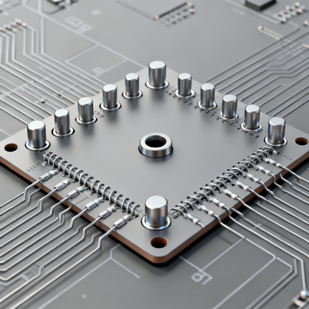
When changing between planes of the same net, place a stitching via directly next to the signal via. This provides a direct, low-inductance path for the return current. Place the stitching via within 20 mils of the signal via. For very high speeds (>5 Gbps), use multiple stitching vias in a fence around the signal via.
Solution 3: Optimize the Stitching Capacitor
When changing between different nets, you must use a capacitor. Use a value with low impedance at your signal’s operating frequency—for high-speed signals (100 MHz+), use 1nF or 100pF capacitors with lower ESL. Use the smallest package possible (0201 or 0402) to minimize ESL and loop area. Place the capacitor directly adjacent to the signal via with traces shorter than 30 mils. Use multiple capacitors in parallel for wider frequency range coverage. The most advanced technique is via-in-pad for the capacitor, eliminating the trace entirely.
Detection and Measurement Methods
Time Domain Reflectometry (TDR)
A TDR measurement shows a sharp impedance dip or spike at the location of the via and capacitor when return path PCB design forces current through a capacitor. If the impedance drops below 50 Ohms, you have a poor return path.
Electromagnetic Field Simulation
Use a 3D EM solver to visualize current density. You will see the current squeezing through the capacitor, creating a high-density current loop. The simulation will also predict radiated emissions.
Near-Field Probe Scanning
Use a near-field magnetic probe to scan the PCB. You will detect a strong magnetic field hotspot around the via and capacitor, indicating the loop antenna.
| Parameter | Optimal Value | Impact on Return Path |
|---|---|---|
| Capacitor Value | 100pF – 1nF | Lower ESL for high-frequency return path |
| Package Size | 0201 or 0402 | Minimizes loop area and inductance |
| Placement Distance | <30 mils from via | Reduces return path loop area |
| Number of Capacitors | 2-3 in parallel | Wider frequency range coverage |
FAQ: Return Path PCB Design Forces Current Through a Capacitor
What happens when return path PCB design forces current through a capacitor?
When return path PCB design forces current through a capacitor, it creates an impedance discontinuity, increases loop area for EMI radiation, and can cause common-mode current generation. The capacitor’s ESL and ESR introduce signal degradation, timing errors, and potential power integrity issues in high-speed PCB systems.
How does forcing return current through a capacitor affect signal integrity?
Forcing return current through a capacitor causes signal reflections, ringing, and insertion loss due to the impedance mismatch. The inductive path slows the return current response, blurring rise times and reducing timing margins for high-speed interfaces like PCIe and DDR.
What is the best way to avoid forcing return current through a capacitor?
The best solution is using a continuous reference plane where signal layers always reference the same ground plane. If layer changes are necessary, use stitching vias for same-net transitions. For different-net transitions, optimize the stitching capacitor with small package size, close placement, and multiple parallel capacitors.
How can I detect if my PCB has a poor return path through a capacitor?
Use Time Domain Reflectometry (TDR) to measure impedance dips at via and capacitor locations. Electromagnetic field simulation can visualize current density hotspots. Near-field probe scanning can detect magnetic field hotspots indicating loop antennas.
What capacitor value is best for high-speed return path stitching?
For high-speed signals above 100 MHz, use 100pF to 1nF capacitors with low ESL. These provide lower impedance at high frequencies compared to standard 0.1uF decoupling capacitors. Use the smallest package size available (0201 or 0402) to minimize parasitic inductance.
Professional Terminology Explained
- ESL (Equivalent Series Inductance): The parasitic inductance inherent in a capacitor, which increases impedance at high frequencies and degrades return path performance.
- Loop Area: The physical area enclosed by the signal path and its return path. Larger loop areas increase inductance and EMI radiation.
- Common-Mode Current: Current that flows in the same direction on both conductors of a differential pair, often caused by return path discontinuities.
- Stitching Via: A via connecting two reference planes of the same net, providing a low-inductance return path for high-speed signals.
Why Choose Our High-Speed PCB Manufacturing
Our advanced fabrication processes support fine-pitch components, controlled impedance, and optimized stackups that help you avoid return path pitfalls. We specialize in manufacturing high-speed PCBs designed to meet stringent signal integrity requirements, ensuring your designs perform reliably at high frequencies.