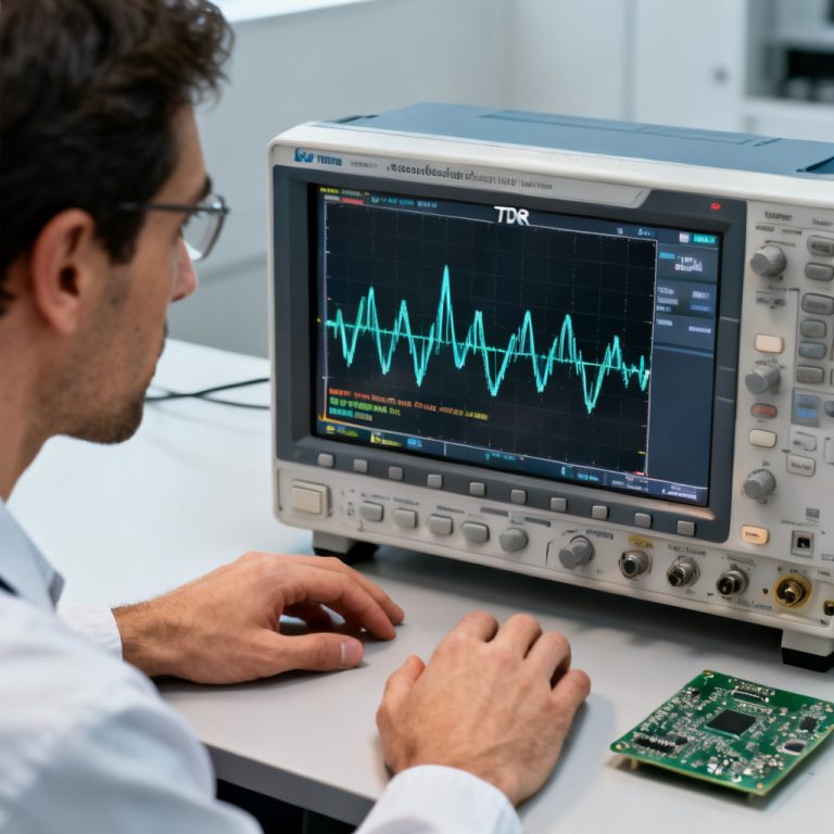
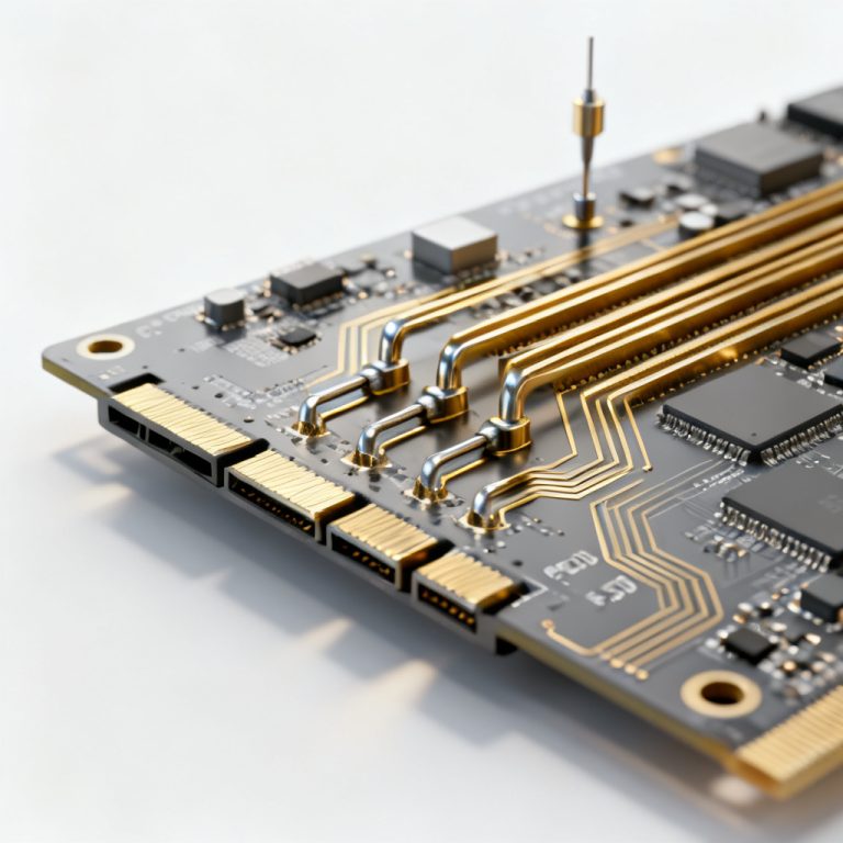
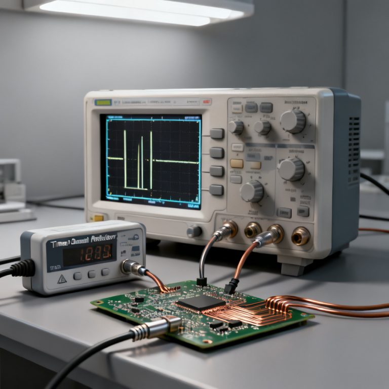
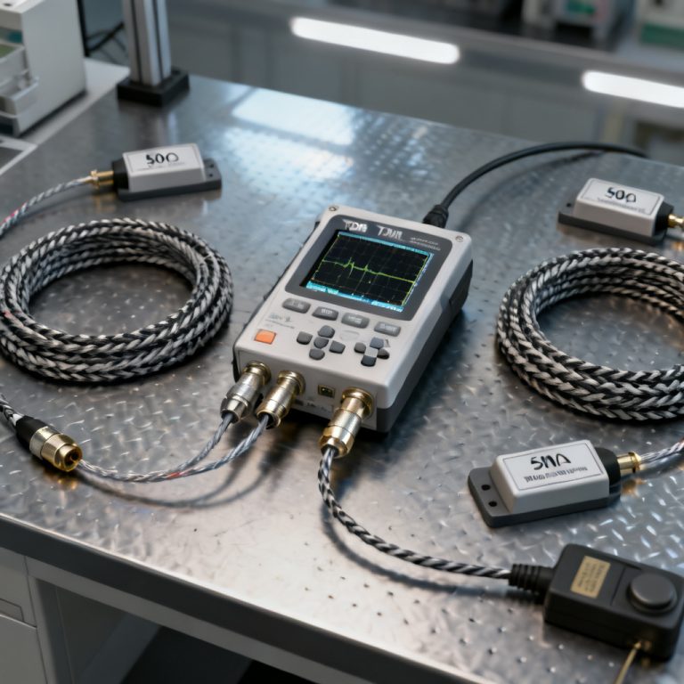
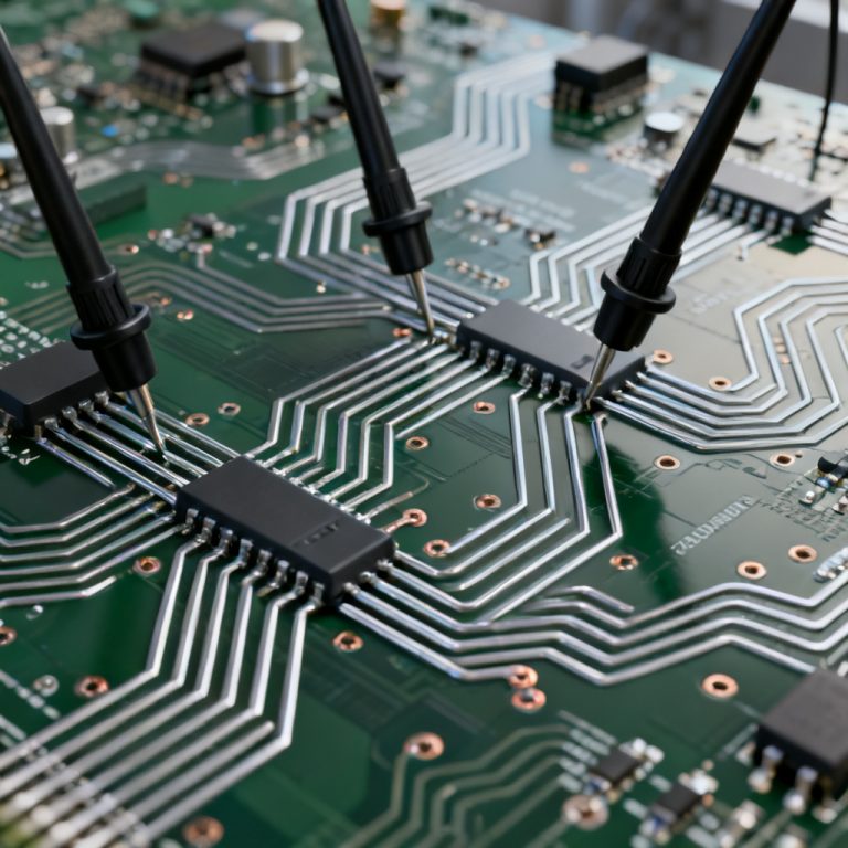
In high-speed PCB design, measuring return path impedance with a Vector Network Analyzer (VNA) is essential for verifying signal integrity. This guide covers the complete process from test coupon design to result interpretation, ensuring your high-speed PCB meets performance requirements.
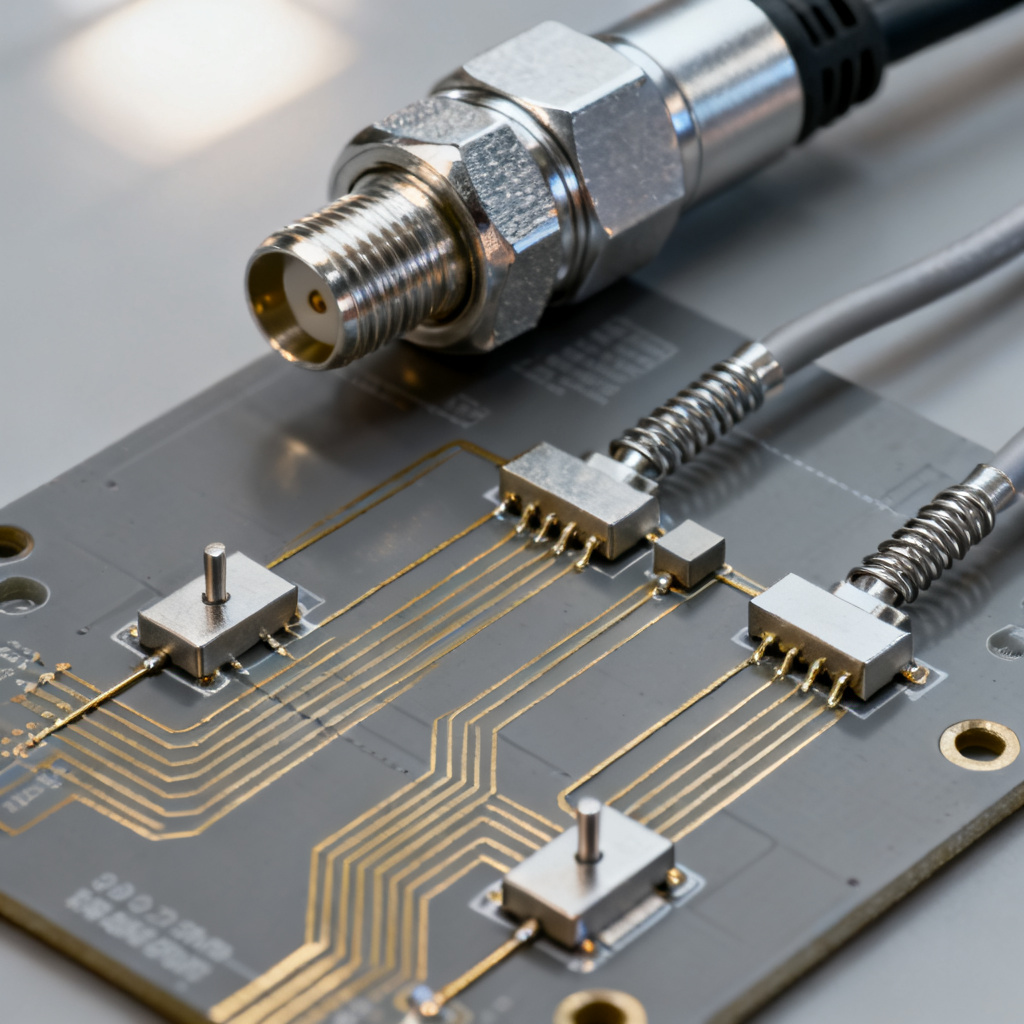
1. Understanding the Physics – What a VNA Measures in the Return Path
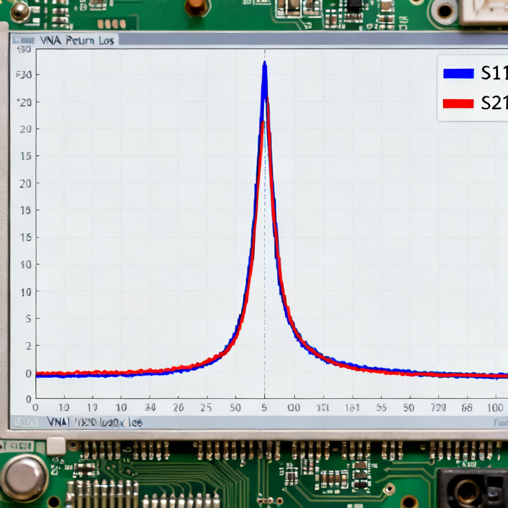
Return path impedance measurement with a VNA focuses on S-parameters: S11 (return loss) and S21 (insertion loss). A low S11 indicates a continuous return path, while high S11 reveals discontinuities like ground plane gaps or poor via stitching. At high frequencies, the return path follows the path of least inductance, making a solid reference plane critical.
1.1 AC Impedance vs. DC Resistance
Return path impedance is frequency-dependent. Above 1 MHz, current seeks the lowest inductance path, not the lowest DC resistance. This is why a solid ground plane minimizes loop inductance and maintains consistent impedance.
1.2 Deriving Z_loop from S11
The VNA measures the total loop impedance (Z_loop) of the signal-return pair. Using the formula Z_loop = Z0 × (1 + S11) / (1 – S11), a flat Z_loop curve indicates a good return path. Any spikes in Z_loop correspond to return path discontinuities.
2. Designing the Test Coupon for Return Path Verification
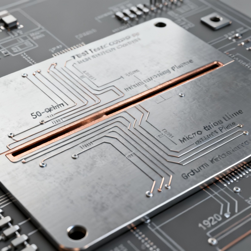
A dedicated test coupon is required for accurate return path impedance measurement. The coupon must include a 50-ohm thru-line and intentional discontinuity structures for verification.
2.1 Thru-Line Coupon
Create a 50-ohm microstrip or stripline trace of known length (e.g., 4 inches) terminated with precision SMA connectors. This provides a baseline for calibration and measurement.
2.2 Return Path Challenge Coupon
Design coupons with specific discontinuities: a ground plane gap, a via stitching test (2 vs. 10 ground vias), or a split plane crossing with stitching capacitors. These reveal how return path impedance changes under real-world conditions.
2.3 Trace Geometry and Termination
Calculate trace width for exactly 50 ohms relative to the reference plane. Use the same dielectric material as the production board. Terminate the far end with a 50-ohm load to avoid open/short distortions.
3. VNA Calibration – The Absolute Prerequisite
Proper calibration moves the VNA’s reference plane to the probe tips or connector edges, ensuring return path impedance measurements are accurate.
3.1 SOLT Calibration
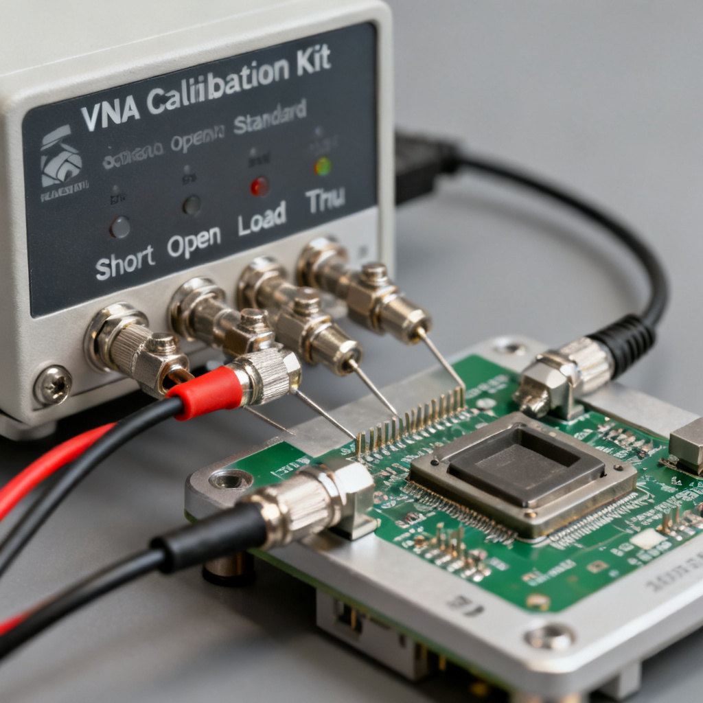
Use Short, Open, Load, Thru standards at the connector interface. This is the standard 2-port calibration for coaxial connectors and provides reliable results up to 40 GHz.
3.2 TRL Calibration
For millimeter-wave frequencies, Thru-Reflect-Line calibration offers higher accuracy. It requires custom standards on the PCB but eliminates connector repeatability errors.
3.3 De-embedding the Launch
Use the 2x-Thru de-embedding technique to remove parasitic effects of the connector launch. This reveals the pure return path impedance of the trace itself.
4. Step-by-Step Measurement Procedure
Follow this procedure to measure return path impedance with a VNA for PCB design verification.
4.1 Setup and Connection
Connect the VNA to the test coupon using phase-stable cables. Set the frequency range from DC to the 5th harmonic of your operating frequency. Use 1601 or 3201 points with an IF bandwidth of 1 kHz.
4.2 Perform Calibration
Execute SOLT or TRL calibration. Verify by connecting a 50-ohm load; S11 should be below -40 dB across the band.
4.3 Measure the Thru-Line Baseline
Record S11 and S21 for the good thru-line. A smooth S11 below -20 dB and monotonic S21 indicate a healthy return path impedance.
4.4 Measure the Challenge Coupon
Connect the challenge coupon. Look for sharp S11 peaks corresponding to return path discontinuities. Convert S11 to Z_loop to quantify the impedance spike.
4.5 Time Domain Analysis (TDR-like)
Use the VNA’s inverse FFT to generate a time-domain impedance plot. A flat line at 50 ohms confirms good return path impedance. Upward spikes indicate inductive discontinuities like ground plane gaps.
5. Interpreting Results and Troubleshooting Common Issues
Understanding measurement artifacts is key to improving return path impedance in high-speed PCB designs.
5.1 High S11 at Low Frequencies
Cause: Poor DC connection in the return path. Fix: Add more ground vias or improve copper plating.
5.2 Periodic Ripple in S21
Cause: Resonance between the trace and a cavity in the ground plane. Fix: Use a solid, continuous ground plane without cutouts.
5.3 Z_loop Spike at Wrong Frequency
Cause: Physical dimensions of the discontinuity differ from simulation. Fix: Measure actual gap width or via spacing and re-simulate.
5.4 Noisy Measurement
Cause: Poor calibration, loose connectors, or high IF bandwidth. Fix: Re-calibrate, tighten connectors to specified torque, and reduce IF bandwidth to 100 Hz.
6. Best Practices for High-Speed PCB Design Verification
Based on expert sources, these best practices ensure reliable return path impedance measurement.
| Practice | Description |
|---|---|
| Design for Testability | Include a dedicated test coupon with thru-line and challenge structures. |
| Calibration is King | Always perform SOLT or TRL calibration before measurement. |
| De-embed Aggressively | Use 2x-Thru method to remove connector effects. |
| Use Time Domain | TDR plots reveal exact physical location of discontinuities. |
| Correlate with Simulation | Compare measured Z_loop with 3D EM simulation results. |
| Document Threshold | Define pass/fail criteria, e.g., Z_loop < 70 ohms up to 40 GHz. |

7. Frequently Asked Questions
What is return path impedance in PCB design?
Return path impedance is the AC impedance of the current return path for a high-speed signal. It must be low and continuous to maintain signal integrity.
How does a VNA measure return path impedance?
A VNA measures S11 (reflection coefficient) and converts it to Z_loop using the formula Z_loop = Z0 × (1 + S11) / (1 – S11). This reveals discontinuities in the return path impedance.
Why is return path impedance important for high-speed PCBs?
Poor return path impedance causes common-mode noise, EMI, and signal degradation. Measuring it ensures your PCB design meets signal integrity requirements.
What is the difference between TDR and VNA for return path measurement?
TDR provides direct time-domain impedance vs. distance. VNA measures frequency-domain S-parameters and can transform to time domain via IFFT. Both are effective for return path impedance verification.
How do I design a test coupon for return path impedance?
Include a 50-ohm thru-line with SMA connectors, plus challenge coupons with intentional discontinuities like ground plane gaps or via arrays. This allows direct return path impedance measurement.
Why Choose Our High-Speed PCB Services?
We provide in-house VNA measurement up to 67 GHz for return path impedance verification. Our test reports include Z_loop plots and TDR analysis, giving you confidence in your high-speed PCB design. Unlike generic PCB manufacturers, we offer dedicated test coupons and de-embedding services to ensure accurate results.