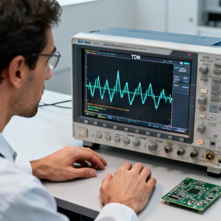
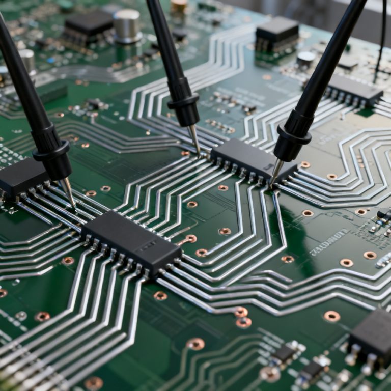
In modern high-speed digital design, achieving reliable data transmission beyond 1 Gbps is no longer solely about logic levels and timing margins. The physical channel—the PCB traces, vias, connectors, and cables—becomes a lossy, frequency-dependent transmission line. Two of the most insidious signal integrity (SI) phenomena that degrade performance are Data Dependent Jitter and ISI in high speed PCB. These are not random; they are deterministic, pattern-dependent errors directly caused by channel loss and signal reflections. Understanding their root causes, measurement, and mitigation is critical for any B2B PCB manufacturer or designer aiming to deliver high-speed, reliable products.
This pillar content synthesizes the most authoritative knowledge from leading industry sources, providing a complete, non-redundant guide to DDJ, ISI, and their relationship with channel imperfections. We will explore the physics, measurement techniques, simulation methods, and practical design rules to minimize these effects in your next high-speed PCB project.
Fundamentals of Data Dependent Jitter and ISI in High Speed PCB
Defining Data Dependent Jitter (DDJ)
DDJ is a type of deterministic jitter (DJ) that correlates directly with the specific bit sequence being transmitted. Unlike random jitter (RJ), which is Gaussian and unbounded, DDJ has a bounded peak-to-peak value. It arises because the channel’s response to a previous bit affects the timing of the current bit. The most common forms of DDJ include:
- Intersymbol Interference (ISI): The dominant contributor. ISI occurs when the energy from a previous bit (or bits) bleeds into the current bit decision time. For example, a long string of identical bits (e.g., 1111) charges the channel capacitance to a high voltage. When a transition occurs (1→0), the signal may not fully discharge to the zero level before the next sampling point, shifting the zero-crossing timing. Conversely, a single 1 after a long string of 0s may not fully charge, causing a later crossing.
- Duty Cycle Distortion (DCD): A special case where the jitter depends on whether the bit is a 1 or a 0, often due to asymmetric rise/fall times or threshold offsets. While DCD is also data-dependent, it is typically addressed separately in jitter decomposition.
Defining Intersymbol Interference (ISI)
ISI is the root mechanism behind most DDJ. It describes the phenomenon where a transmitted symbol (bit) is smeared in time due to the limited bandwidth of the channel. The channel acts as a low-pass filter, attenuating high-frequency components (sharp edges) while preserving low-frequency components (long runs). Key characteristics:
- Pulse Broadening: A sharp digital pulse becomes a rounded, stretched waveform.
- Residual Energy: After the intended bit period, a fraction of the signal’s energy remains, interfering with subsequent bits.
- Pattern Dependence: The worst-case ISI occurs when a transition is preceded by many identical bits (e.g., 000…01 or 111…10). This is because the channel has had time to charge/discharge to the maximum level, and the subsequent transition must overcome the largest possible voltage swing.
The Direct Link: Channel Loss Causes ISI
Channel loss is the primary physical cause of ISI. Loss comes in two forms:
- Conductor Loss (Skin Effect): At high frequencies, current flows only on the surface of copper traces, increasing resistance. Skin effect loss scales with √f (square root of frequency).
- Dielectric Loss: The insulating material (e.g., FR-4, Megtron, Rogers) absorbs energy from the electric field. Dielectric loss scales linearly with frequency and is characterized by the dissipation factor (Df or tan δ).
A lossy channel acts as a low-pass filter. When a high-speed signal (containing both low-frequency data patterns and high-frequency edges) propagates, the high-frequency components are attenuated more than the low-frequency components. This frequency-dependent attenuation distorts the waveform, causing the slow rise/fall times that lead to ISI.
Reflections: The Second Major Cause of DDJ in High Speed PCB
While channel loss is a distributed effect, reflections are a localized phenomenon caused by impedance discontinuities. Any change in the characteristic impedance (Z0) of the transmission line—at vias, connectors, component pads, or trace width changes—creates a partial reflection of the signal.
How Reflections Create Jitter
A reflected wave travels back toward the source, and if the source impedance is not matched, it re-reflects. This forward-traveling reflected wave arrives at the receiver at a delayed time, superimposing on the main signal. The effect on jitter is twofold:
- Voltage Overshoot/Undershoot: The reflected voltage adds to or subtracts from the main signal, shifting the zero-crossing point. For a rising edge, a positive reflection causes an earlier crossing; a negative reflection causes a later crossing.
- Post-Cursor and Pre-Cursor ISI: Reflections create “echoes” of past bits (post-cursor ISI) and, in severe cases, even affect bits before the main transition (pre-cursor ISI) if the reflection path is long enough.
The Role of Stubs and Vias
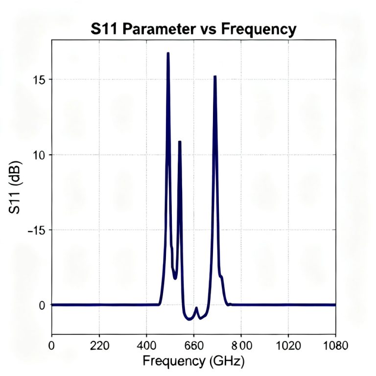
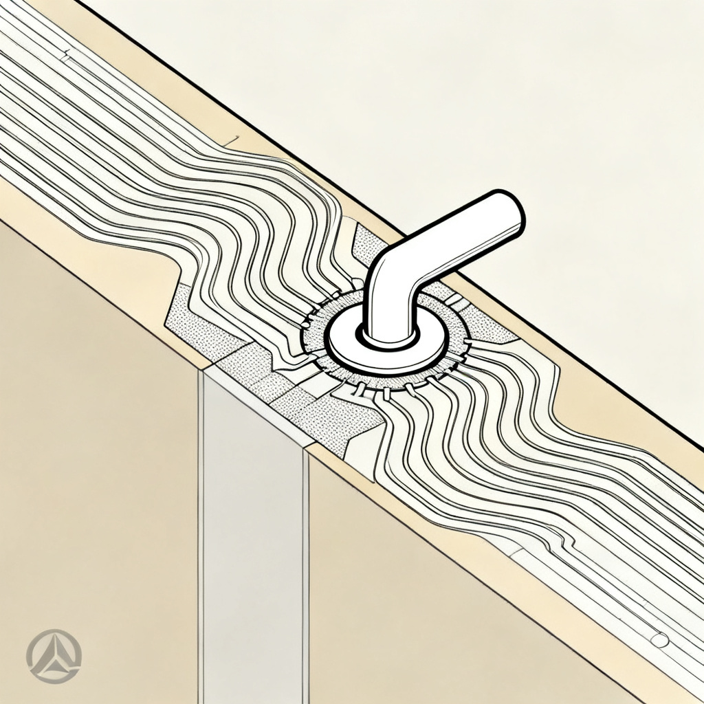
Stubs (unused portions of a via or trace) are particularly problematic. A via stub acts as a resonant cavity at certain frequencies (quarter-wavelength resonance). At these frequencies, the stub reflects almost all the signal energy back, creating deep notches in the channel’s frequency response (S21). These notches severely distort the signal, increasing both ISI and DDJ.
Impedance Matching and Termination
Proper termination is the primary defense against reflections. Common strategies include:
- Source Series Termination: A resistor at the driver matches the driver’s output impedance to the transmission line.
- Parallel Termination: A resistor at the receiver pulls the line to a termination voltage (Vtt).
- AC Termination: A resistor and capacitor in series at the receiver, useful for reducing DC power consumption.
For high-speed serial links (e.g., PCIe, USB, Ethernet), on-die termination (ODT) is standard, but PCB design must ensure that the trace impedance (single-ended or differential) matches the specified value (e.g., 50Ω single-ended, 100Ω differential).
Measurement and Characterization of DDJ and ISI in High Speed PCB
To quantify the severity of DDJ and ISI, engineers use specialized test equipment and metrics.
Eye Diagram Analysis
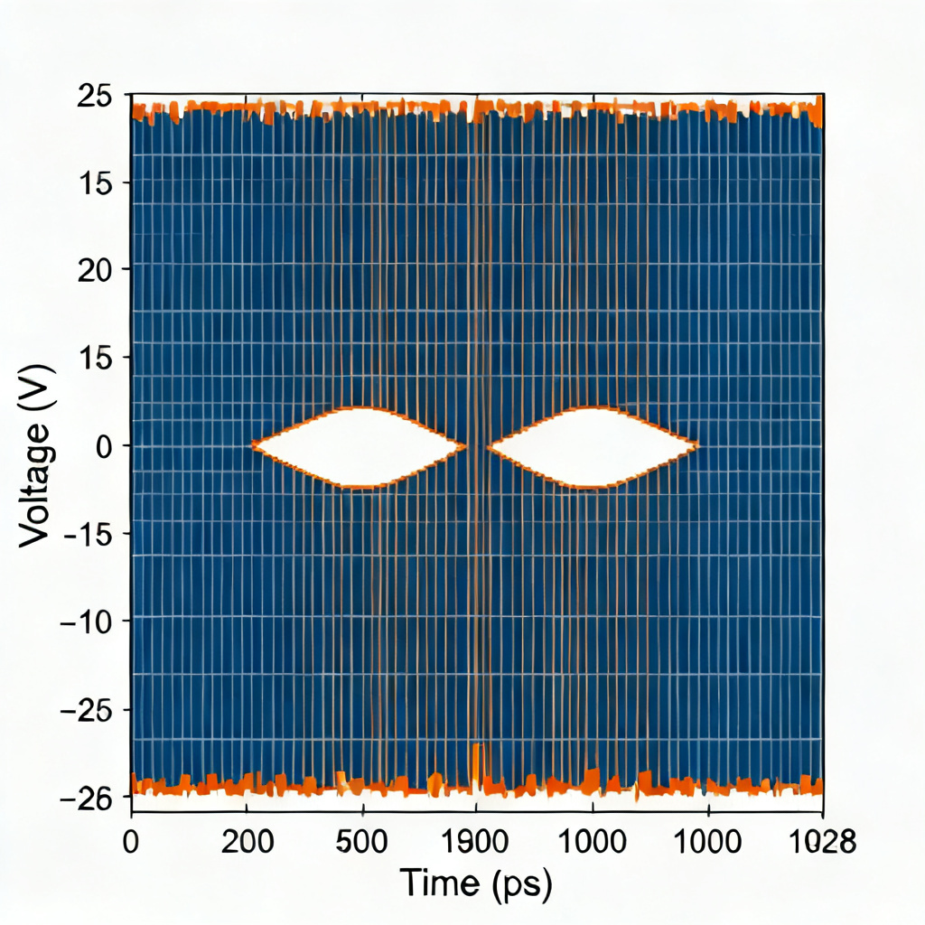
The eye diagram is the most intuitive tool. It overlays many bits of a signal, triggered on the data clock.
- Eye Closure: ISI and DDJ cause the eye to close vertically (voltage margin reduction) and horizontally (timing margin reduction).
- Deterministic Jitter (DJ) Measurement: The horizontal eye opening at the center of the eye (where the bit is sampled) is reduced by DJ. A bathtub curve plot (bit error rate vs. sampling point) separates RJ (sloping tails) from DJ (flat plateau).
- Mask Testing: Industry standards (e.g., USB, PCIe) define a mask region inside the eye. Any violation indicates a signal integrity failure, often due to excessive ISI or reflections.
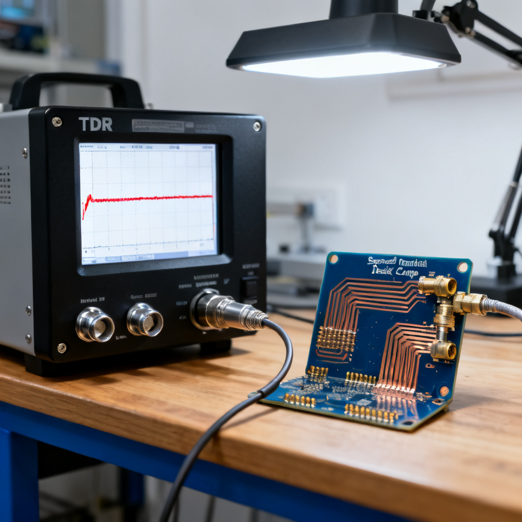
Time Domain Reflectometry (TDR) and Time Domain Transmission (TDT)
TDR sends a fast step pulse into the channel and measures the reflected voltage. It reveals the location and magnitude of impedance discontinuities. TDT measures the transmitted pulse, showing the overall rise time degradation and loss.
- TDR for Reflections: A rising impedance (e.g., a narrow trace) produces a positive reflection; a falling impedance (e.g., a via pad) produces a negative reflection.
- TDT for ISI: The transmitted pulse’s rise time is a direct indicator of channel bandwidth. A slower rise time implies greater high-frequency loss and thus more ISI.
Channel Operating Margin (COM)
For advanced standards like IEEE 802.3 (Ethernet) and PCIe, COM is a figure of merit that predicts the link’s ability to operate with a given channel, including the effects of ISI, crosstalk, and reflections. It is computed from S-parameter measurements (S11, S22, S21, S12) and incorporates equalization assumptions.
Bit Error Rate Testing (BERT)
The ultimate test: a BERT sends a known pseudo-random bit sequence (PRBS) and counts errors. By varying the sampling point (horizontal and vertical), a BERT can produce a bathtub curve and directly measure the total jitter (TJ) at a given BER (e.g., 10^-12).
Mitigation Strategies for Data Dependent Jitter and ISI in High Speed PCB
Low-Loss Material Selection
- FR-4 is inadequate above ~5 Gbps. Its high dissipation factor (Df ~0.02) causes severe dielectric loss.
- Mid-Loss Materials (e.g., Megtron 4, TU-872 SLK): Df ~0.008–0.012, suitable for 10–25 Gbps.
- Low-Loss Materials (e.g., Megtron 6, Rogers 3000/4000 series): Df ~0.002–0.005, necessary for 25+ Gbps and high-reliability applications.
Pre-Emphasis and Equalization
Since the channel distorts the signal, we can pre-distort it at the transmitter or correct it at the receiver.
- Transmitter Pre-Emphasis (De-Emphasis): The driver boosts the high-frequency content (the first bit after a transition) relative to the subsequent bits. This compensates for the channel’s low-pass nature.
- Receiver Equalization (CTLE, DFE): A Continuous-Time Linear Equalizer (CTLE) amplifies high frequencies. A Decision Feedback Equalizer (DFE) subtracts the ISI contributions of previously received bits from the current bit sample.
Impedance Control and Via Optimization
- Controlled Impedance: Ensure trace width, dielectric thickness, and copper weight are precisely controlled to achieve the target Z0. Work with your PCB manufacturer to define stackup and tolerances.
- Backdrilling: Remove unused via stubs by drilling out the non-functional barrel portion. This eliminates quarter-wave resonances.
- Via Stitching: Use multiple ground vias adjacent to signal vias to reduce inductance and improve return path.
- Avoid 90° Corners: Use 45° chamfered corners or curved traces to minimize impedance discontinuity.
Layout and Routing Best Practices
- Minimize Trace Length: Shorter traces mean less loss and fewer reflections.
- Maintain Return Path Integrity: Ensure a continuous ground plane beneath high-speed traces. Avoid slots or splits in the plane.
- Differential Pair Routing: For high-speed serial links, keep differential pairs tightly coupled (edge-to-edge spacing = trace width) and length-matched.
- Avoid Stubs on Main Traces: Any branch or stub (e.g., for a test point) must be kept as short as possible (typically < 100 mils).
Simulation and Modeling
Before fabrication, simulate the channel using 3D electromagnetic (EM) solvers (e.g., Ansys HFSS, Keysight ADS, CST) or 2D field solvers (e.g., Polar SI9000). Extract S-parameters and run transient simulations with a PRBS pattern to predict eye diagrams and jitter.
- Correlation: Validate simulation results with TDR/TDT measurements on test coupons.
- What-If Analysis: Simulate the effect of different materials, trace widths, via structures, and termination values.
Case Studies and Practical Examples
Case Study 1: 10 Gbps NRZ Link on FR-4
A 20-inch trace on standard FR-4 shows an eye diagram that is nearly closed. TDR reveals no major reflections, but TDT shows a rise time of 150 ps (vs. 35 ps at the source). The channel’s -3 dB bandwidth is only 2.3 GHz. The dominant jitter is ISI from dielectric loss. Solution: Switch to a mid-loss material (e.g., Megtron 4) and add a CTLE at the receiver. The eye opens to 40% of the unit interval.
Case Study 2: 25 Gbps Link with Via Stub Resonance
A 25 Gbps NRZ link experiences random bit errors at a specific data pattern (e.g., 1010…). Eye diagram shows a double-lobe structure. S21 measurement reveals a deep notch at 12.5 GHz. TDR shows a 120-mil via stub. Solution: Backdrill the vias to remove the stub. The notch disappears, and the eye diagram becomes clean. The bit error rate drops from 10^-6 to below 10^-12.
Case Study 3: Reflection from a Connector
A high-speed connector on a backplane causes a 15% impedance mismatch. The resulting reflection creates a 20 ps DDJ component on the rising edge. Simulation shows that adding a series termination resistor (22Ω) at the driver and a parallel termination (50Ω to Vtt) at the receiver reduces the DDJ to 5 ps.
Material Comparison for Data Dependent Jitter and ISI in High Speed PCB
| Material Type | Dissipation Factor (Df) | Max Data Rate (NRZ) | Relative Cost | Application |
|---|---|---|---|---|
| Standard FR-4 | ~0.02 | <5 Gbps | Low | Low-speed digital |
| Mid-Loss (Megtron 4) | 0.008–0.012 | 10–25 Gbps | Medium | High-speed serial links |
| Low-Loss (Rogers 3000) | 0.002–0.005 | 25+ Gbps | High | RF, microwave, high-reliability |
FAQ: Data Dependent Jitter and ISI in High Speed PCB
What is the main cause of Data Dependent Jitter in high speed PCB?
The main cause of Data Dependent Jitter in high speed PCB is channel loss (skin effect and dielectric loss) which leads to Intersymbol Interference (ISI), and signal reflections from impedance discontinuities.
How does channel loss contribute to ISI in high speed PCB?
Channel loss acts as a low-pass filter, attenuating high-frequency components of the signal, which slows rise/fall times and causes residual energy from previous bits to interfere with the current bit, creating ISI.
What are effective ways to reduce DDJ in high speed PCB design?
Effective ways to reduce DDJ in high speed PCB design include using low-loss materials, implementing pre-emphasis and equalization, optimizing impedance control, backdrilling vias, and proper termination.
How do reflections cause jitter in high speed PCB?
Reflections from impedance mismatches (e.g., vias, connectors) create delayed echoes that superimpose on the main signal, shifting zero-crossing points and causing deterministic jitter.
What role does via stub play in ISI for high speed PCB?
Via stubs create quarter-wave resonances that cause deep notches in the channel frequency response, significantly increasing ISI and DDJ if not backdrilled.
Conclusion: Achieving Signal Integrity in High Speed PCB Design
Data Dependent Jitter and ISI are not abstract concepts; they are the practical consequences of a lossy, imperfect channel. For any B2B PCB manufacturer or design house, mastering the interplay between channel loss (skin effect and dielectric loss) and reflections (impedance discontinuities) is essential to delivering high-speed products that meet stringent performance standards.
The path to success involves:
- Understanding the Physics: Recognize that every trace, via, and connector is a contributor to jitter.
- Characterizing the Channel: Use TDR, TDT, and S-parameter measurements to quantify loss and reflections.
- Simulating Before Building: Leverage EM simulation to predict performance and optimize design.
- Implementing Robust Mitigation: Choose low-loss materials, control impedance, optimize vias, and apply equalization.
- Validating with Testing: Use eye diagrams, BERT, and COM to confirm that the link meets the required margin.
By following these principles, you can design high-speed PCBs that minimize DDJ and ISI, ensuring reliable data transmission even at multi-gigabit rates. For complex projects, partner with a PCB manufacturer that offers advanced material options, controlled impedance fabrication, and signal integrity simulation support.
Call to Action for B2B Buyers: Are you designing a high-speed PCB that requires low jitter and robust signal integrity? Our team specializes in advanced PCB fabrication with low-loss materials, controlled impedance, and backdrilling capabilities. Contact us today for a free signal integrity consultation and quote. Let us help you turn your high-speed design into a reliable product.