[rank_math_breadcrumb]
Master jitter decomposition for High Speed PCB serial data links. This comprehensive step-by-step guide covers TIE, RJ, DJ, PJ, ISI, DCD, and BER eye diagrams using industry-standard methodologies (NQ-Scale, Tail-Fit, Spectrum). Perfect for B2B PCB engineers and designers.
1. Why Jitter Decomposition is Critical for High Speed PCB
In modern High Speed PCB design (e.g., PCIe Gen 4/5, USB 3.2, 10G Ethernet, SerDes), the timing margin is shrinking. A signal’s transition from a logic 0 to a logic 1 must arrive at the receiver within a precise window. Jitter – the deviation of a signal’s edge from its ideal timing position – is the primary enemy of signal integrity.
Jitter decomposition is the process of separating total jitter (TJ) into its deterministic (DJ) and random (RJ) components. This is not just an academic exercise; it is the only way to identify the root cause of bit errors in your PCB design. Without decomposition, you cannot distinguish between a power supply noise issue (Periodic Jitter) and a crosstalk issue (Data-Dependent Jitter).
This step-by-step guide integrates the most trusted industry methodologies from leading test equipment manufacturers (Teledyne LeCroy, Keysight, Rohde & Schwarz) to give you a definitive, actionable workflow for High Speed PCB jitter analysis.
2. The Physics of Jitter: Understanding the Root Causes
Before diving into the step-by-step process, you must understand what jitter components you are looking for. Jitter is broadly categorized into two families:
2.1 Random Jitter (RJ) in High Speed PCB
Random Jitter in a High Speed PCB originates from thermal noise, shot noise, and flicker noise in semiconductor junctions. It is characterized by a Gaussian (unbounded) distribution. It has no pattern and is additive. In the time domain, it appears as a white noise floor.
Its impact is unbounded – meaning it can theoretically cause a bit error at any time, though the probability decreases with amplitude. RJ is the fundamental limit to your PCB’s Bit Error Rate (BER). The key measurement for RJ in jitter decomposition is its RMS value (sigma, σ).
2.2 Deterministic Jitter (DJ) in High Speed PCB
Deterministic Jitter in High Speed PCB originates from specific, identifiable design flaws. It is characterized as bounded (has a finite peak-to-peak value) and is correlated to the data pattern or system clocks.
Its sub-components include:
- Data-Dependent Jitter (DDJ): Includes Intersymbol Interference (ISI) caused by bandwidth limitations of the PCB trace (lossy dielectrics, impedance mismatches) and Duty Cycle Distortion (DCD) caused by a threshold offset in the receiver or asymmetry in the driver’s rise/fall times.
- Periodic Jitter (PJ): Caused by switching power supply noise, electromagnetic interference (EMI) from nearby clocks, or crosstalk from aggressor signals. It appears as sinusoidal jitter.
- Bounded Uncorrelated Jitter (BUJ): Caused by crosstalk from an uncorrelated aggressor (e.g., a separate clock lane interfering with a data lane).
3. Step-by-Step Jitter Decomposition Workflow
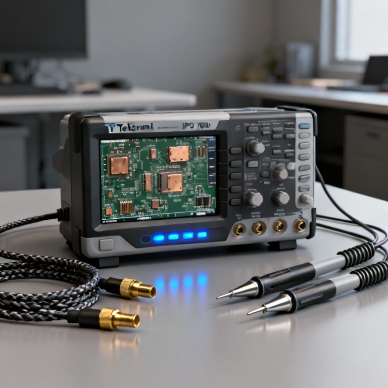
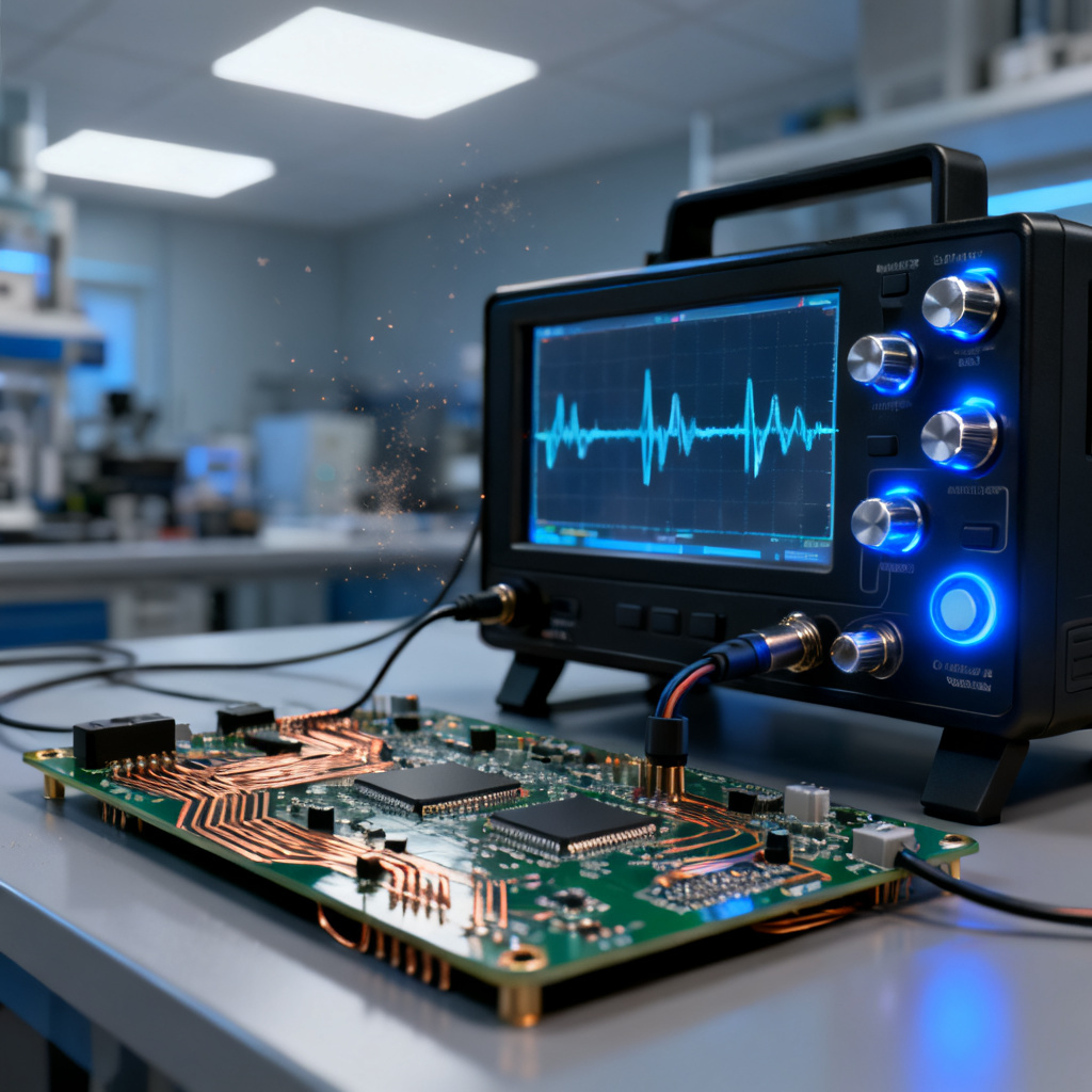
This workflow is adapted from the three top-tier sources. It assumes you have a high-bandwidth real-time oscilloscope (e.g., 20+ GHz for 28 Gbps signals) or a sampling oscilloscope with a jitter analysis software package.
Step 1: Acquire the Serial Data Waveform for Jitter Decomposition
Source Insight (Keysight / Teledyne LeCroy): Use a low-noise, high-bandwidth probe (e.g., InfiniiMax III or WaveLink). Ensure the probe’s bandwidth exceeds the 3rd harmonic of the data rate.
Clock Recovery: This is the most critical initial step. The oscilloscope must perform a Clock Recovery to create a reference clock from the data stream. Use a Phase-Locked Loop (PLL) with a specified loop bandwidth (e.g., 10 MHz for PCIe Gen 3). The PLL mimics the receiver’s clock recovery circuit. The result is an ideal “golden” clock edge location against which to measure jitter.
Step-by-Step Action:
- Connect the probe to the test point (typically a via or test pad at the receiver end of the PCB trace).
- Set the oscilloscope to acquire a long record length (e.g., 10 million points) to capture low-frequency jitter.
- Enable Clock Recovery. Select the appropriate standard (e.g., PCIe, USB, Ethernet) or manually set the PLL bandwidth.
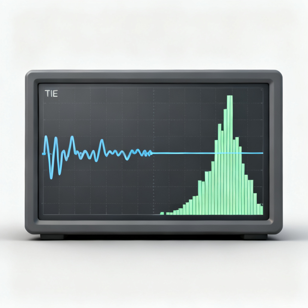
Step 2: Measure Time Interval Error (TIE) for Jitter Analysis
Source Insight (Rohde & Schwarz): TIE is the difference between the actual clock edge position and the ideal position (from the PLL reference). TIE is the fundamental jitter measurement. All subsequent decomposition is based on the TIE track. You cannot decompose jitter from an eye diagram alone.
You will create a “TIE Trend” – a plot of jitter magnitude vs. time (or vs. bit number).
Step-by-Step Action:
- Instruct the oscilloscope software to measure TIE on every rising edge of the recovered clock.
- Export the TIE values as a time series list. This list is your raw data for jitter decomposition.
- Visual Check: Plot the TIE trend. A sinusoidal pattern indicates Periodic Jitter (PJ). A pattern that repeats every 8 bits indicates DDJ (ISI).
Step 3: Separate Random Jitter (RJ) from Deterministic Jitter (DJ) using the Tail-Fit Method
Source Insight (Teledyne LeCroy / Keysight): This is the industry-standard “Dual-Dirac” model. It assumes that the deterministic jitter creates two distinct peaks in the jitter histogram, separated by a distance (DJ), while the random jitter creates the Gaussian tails on each side.
The Process:
- Create a histogram of all TIE measurements.
- Identify the Tails: The outer edges of the histogram (the left and right tails) are assumed to be purely Gaussian (RJ).
- Gaussian Fit: Fit a Gaussian curve to each tail. The standard deviation (σ) of this curve is the RJ RMS value.
- Calculate DJ: The distance between the means of the two Gaussian curves is the DJ (δδ) value.
- Calculate TJ: Total Jitter at a specific BER (e.g., 10^-12) is calculated as: TJ = DJ + 2 * Q(BER) * RJ, where Q(BER) is a constant (e.g., 14 for BER 10^-12).
Step-by-Step Action:
- In your jitter analysis software, select the “Histogram” view of the TIE data.
- Choose the Tail-Fit or Dual-Dirac analysis mode.
- Set the target BER (typically 10^-12 for high-speed serial links).
- Output: The software will display: RJ (rms), DJ (pk-pk), and TJ @ BER.
Step 4: Decompose Deterministic Jitter into DDJ (ISI & DCD) and PJ
Source Insight (Rohde & Schwarz / Keysight): Knowing you have DJ is not enough. You need to know if it is ISI (fix with equalization) or PJ (fix with power supply filtering).
Method 1: Pattern Synchronization (for DDJ): The TIE trend is averaged over many repetitions of a known data pattern (e.g., PRBS7, PRBS15). Random jitter averages to zero, leaving only the pattern-dependent jitter (DDJ). Sub-decomposition includes: DCD (the average jitter on rising edges vs. falling edges) and ISI (the residual pattern-dependent jitter after removing DCD).
Method 2: Spectral Analysis / Jitter Spectrum (for PJ): Perform an FFT on the TIE trend. You will see spectral peaks. Spurs at specific frequencies are Periodic Jitter (PJ). Common frequencies are the switching frequency of your buck converter or the fundamental of a nearby clock. A flat noise floor is Random Jitter (RJ). Pattern-related spurs are DDJ (ISI).
Step-by-Step Action:
- For DDJ: Load a known PRBS pattern. Use the “Pattern Analysis” tool. The software will show you the jitter for each unique bit pattern (e.g., “00001”, “11110”).
- For PJ: Switch to the “Jitter Spectrum” or “FFT” view. Identify the peak frequencies. Note the amplitude of the spurs.
- For BUJ: If you see spurs that do not correlate to your system clock or data rate, they may be BUJ from crosstalk.
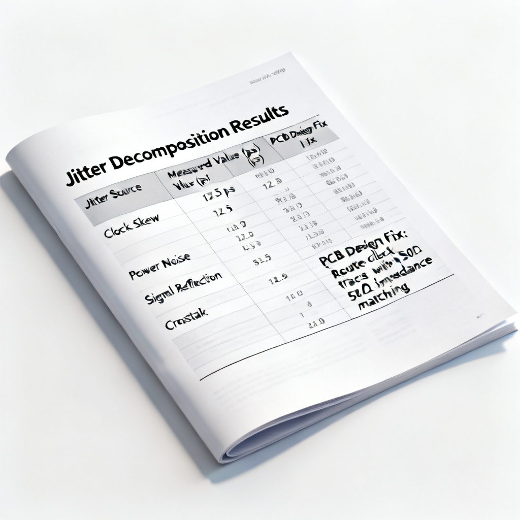
4. Interpreting the Results: From Jitter Decomposition to PCB Design Action
Jitter decomposition is useless without actionable insight. Here is how to translate the numbers into PCB design changes:
| Jitter Component | Root Cause in High Speed PCB | Actionable Fix |
|---|---|---|
| High RJ | Poor VCO phase noise, noisy LDO | Use lower-noise power supplies. Improve PLL loop filter design. |
| High DDJ (ISI) | Lossy transmission line, impedance mismatch, long via stubs | Reduce trace length. Use lower-loss dielectric (e.g., Megtron 6). Add equalization (CTLE, DFE). Optimize via backdrilling. |
| High DCD | Asymmetric driver, incorrect termination, threshold offset | Check driver rise/fall symmetry. Verify termination resistor values. Adjust receiver threshold. |
| High PJ | Switching regulator ripple, EMI from adjacent clock line | Add ferrite beads to power rail. Increase decoupling capacitance. Increase spacing between clock and data traces. |
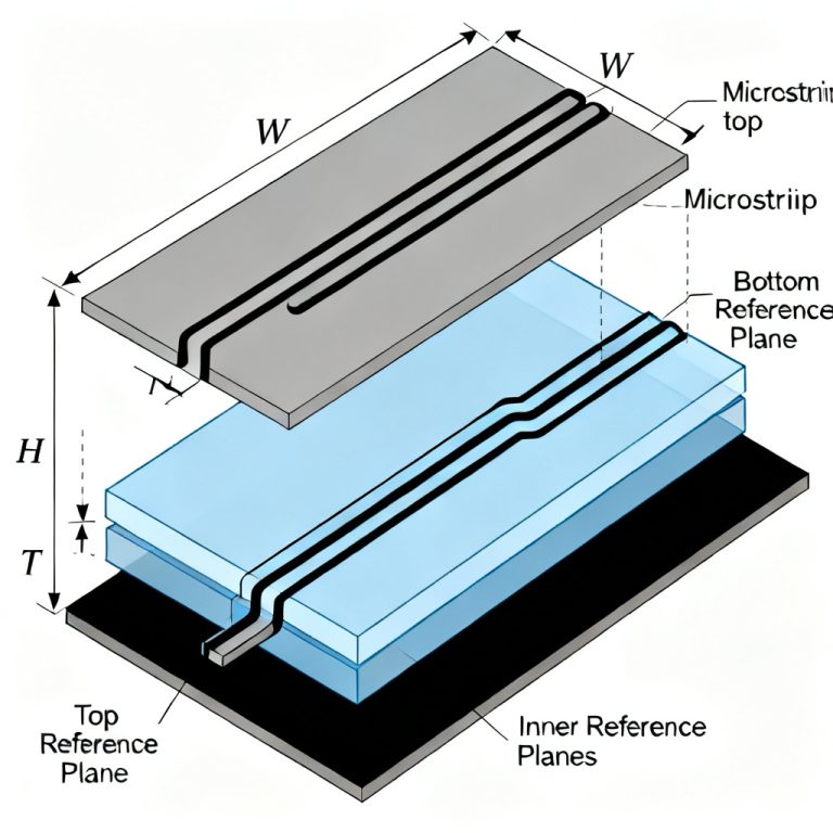
| High BUJ | Crosstalk from an aggressor signal on a different layer | Increase inter-layer spacing. Use stripline (shielded) routing. Add stitching vias. |
5. Common Pitfalls & Best Practices for Jitter Decomposition
Pitfall 1: Using an incorrect PLL bandwidth. Always set the PLL bandwidth to match the receiver’s specification. A bandwidth too high will suppress real low-frequency jitter. A bandwidth too low will include wander (DC drift) as jitter.
Pitfall 2: Confusing RMS with Peak-to-Peak for RJ. Remember: RJ is Gaussian. You cannot measure its true peak-to-peak. Always quote RJ as RMS (σ). Total Jitter (TJ) is the only valid peak-to-peak metric, and it is only valid at a specified BER.
Pitfall 3: Ignoring the measurement noise floor. The oscilloscope itself has jitter. Before measuring your DUT, measure the oscilloscope’s own jitter (short the input). Subtract this from your measurement using root-sum-square (RSS) if the scope’s noise is significant.
Pitfall 4: Decomposing jitter on a closed eye. Jitter decomposition algorithms work best on a partially open eye. If the eye is completely closed, the clock recovery PLL will fail. In that case, use a known PRBS pattern and a clean reference clock first.
6. Conclusion: The Path to a Robust High Speed PCB
Jitter decomposition is not a luxury; it is a mandatory step in the design validation of any high-speed serial link PCB. By following this step-by-step guide—from TIE acquisition to spectral analysis—you move from a vague “the eye looks bad” to a precise diagnosis: “I have 3 ps of ISI at 28 Gbps due to a 6-inch trace on FR4.”
For your B2B high-speed PCB manufacturing and assembly, mastering this analysis allows you to:
- Specify the correct materials (e.g., low-loss laminates for ISI reduction).
- Validate your stackup design (e.g., proper impedance control to minimize DCD).
- Provide customers with detailed jitter reports, proving your PCBs meet the tightest timing margins.
Next Steps: Apply this workflow to your next PCIe Gen 5 or 112G PAM-4 design. The components may be complex, but the logic is linear: Measure TIE → Fit Tails → Decompose DJ → Fix the Root Cause.
This guide was synthesized from industry-leading methodologies. For specific oscilloscope software instructions, refer to your equipment’s manual or contact your test equipment vendor.
Frequently Asked Questions about Jitter Decomposition in High Speed PCB
What is jitter decomposition in High Speed PCB design?
Jitter decomposition is the process of separating total jitter into its random (RJ) and deterministic (DJ) components. In High Speed PCB design, this step-by-step analysis is critical for identifying root causes like ISI, DCD, or PJ, enabling targeted design fixes.
Why is TIE measurement important for jitter decomposition?
Time Interval Error (TIE) is the fundamental measurement for jitter decomposition. It captures the deviation of each signal edge from its ideal timing position, providing the raw data needed for subsequent histogram and spectral analysis in High Speed PCB validation.
How do I separate RJ and DJ during jitter decomposition?
The industry-standard method is the Tail-Fit (Dual-Dirac) approach. By fitting Gaussian curves to the tails of the TIE histogram, you can extract RJ (RMS) and DJ (peak-to-peak). This step-by-step technique is essential for accurate jitter decomposition in High Speed PCB serial data analysis.
What is the role of PLL bandwidth in jitter decomposition?
The PLL bandwidth in clock recovery mimics the receiver’s behavior. Using an incorrect bandwidth can mask or amplify jitter components. For proper jitter decomposition in High Speed PCB, always set the PLL bandwidth per the serial link standard (e.g., 10 MHz for PCIe Gen 3).