Properly sizing power planes and traces for DC drop requirements is essential in high-speed PCB design to maintain voltage integrity and prevent functional failures. This guide provides a comprehensive methodology from industry experts.

Understanding DC Drop Fundamentals for Power Planes and Traces
What Is DC Drop and Why It Matters for Power Planes and Traces Sizing
DC drop (IR drop) is the voltage loss along a power distribution network due to conductor resistance. For power planes and traces, this is calculated using Ohm’s Law: V_drop = I × R. In high-speed designs, even small drops on low-voltage rails (e.g., 1.0V–1.8V) can cause logic errors, making proper power planes and traces sizing critical for performance.
Key Terminology for Power Planes and Traces Sizing
Understanding terms like power plane (continuous copper layer), trace (routed conductor), copper weight (thickness), and current carrying capacity is foundational for power planes and traces sizing. These parameters directly affect resistance and voltage drop.
Step-by-Step Methodology for Power Planes and Traces Sizing
Step 1: Define DC Drop Budget and Current Requirements
Start by defining allowable DC drop per rail. Typical budgets for power planes and traces sizing include 1–3% for core voltage rails and 3–5% for I/O rails. Determine maximum current from datasheets, including peak transient currents (2–5× static). Create a power budget table for all critical power planes and traces.
Step 2: Calculate Required Trace Width for Given Current
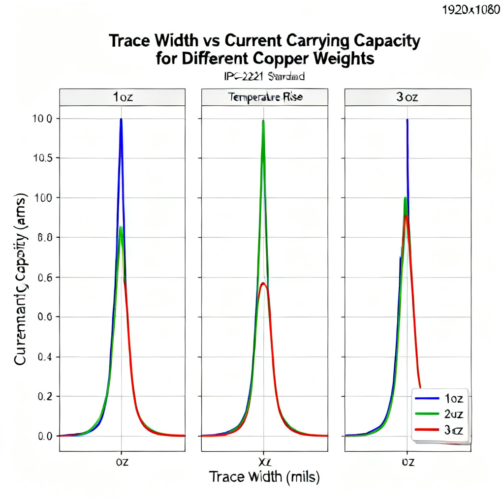
Use the IPC-2221 formula for power planes and traces sizing: I = k × (ΔT)^0.44 × (W × T)^0.725. For external traces, k = 0.048; internal traces use k = 0.024. A practical rule: 1 oz copper, 10°C rise = 1A per 10 mils (external) or 1A per 20 mils (internal). For high-current power planes and traces (>5A), use minimum 2 oz copper and width ≥ 50 mils.
Step 3: Model DC Drop Using Resistance Calculation
Calculate trace resistance: R_trace = (0.5 μΩ·in × L) / (W × T). For power planes, use sheet resistance: 1 oz = 0.5 mΩ/sq, 2 oz = 0.25 mΩ/sq. Use 2D field solvers (e.g., HyperLynx PI) for accurate power planes and traces modeling, considering via resistance and temperature effects.
Step 4: Sizing Power Planes for Low Impedance
For power planes and traces sizing, use dedicated plane layers for each voltage rail. Plane width should be at least 10× trace width. For high-current rails (>10A), use multiple layers in parallel. Stitch vias every 0.1–0.2 inches. For BGA devices, use via-in-pad to reduce power planes and traces resistance.
Step 5: Verification and Simulation
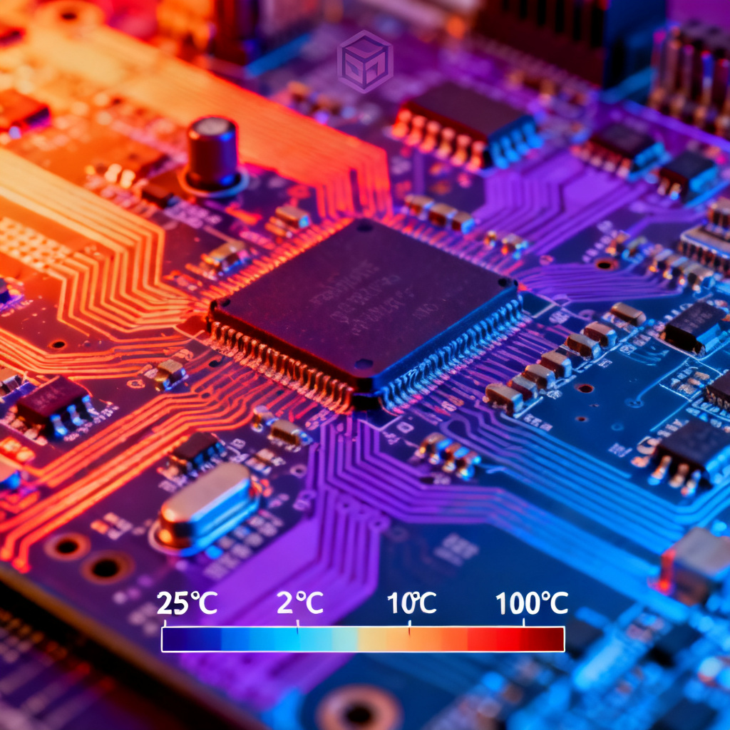
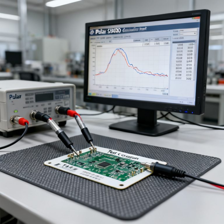
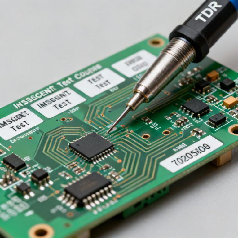
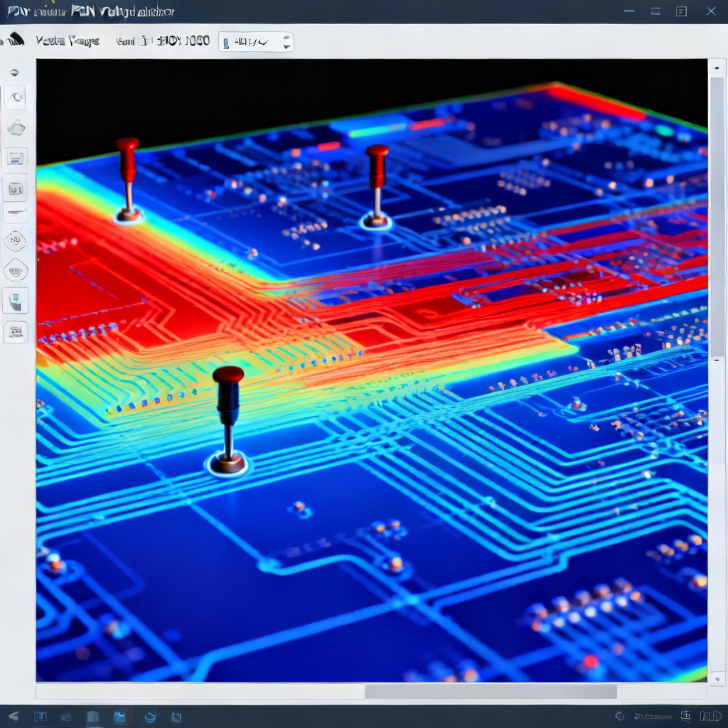
Run DC drop simulation (e.g., Altium PDN Analyzer) to visualize voltage distribution across power planes and traces. Acceptable variation is <5%. Use 4-wire Kelvin probes on prototypes to measure actual DC drop on power planes and traces. Thermal imaging helps detect hot spots from excessive IR drop.
Practical Examples for Power Planes and Traces Sizing
Example 1: Sizing a Trace for a 3.3V Rail at 2A
Using IPC-2221 for power planes and traces sizing: 2A current, 10°C rise, external 1 oz copper yields width ≈ 24 mils (use 30 mils for margin). DC drop = 71.4 mV (2.2% of 3.3V, acceptable).
Example 2: Power Plane for a 1.2V Core at 15A
For power planes and traces sizing at high current: max drop 1% (12 mV) requires plane resistance <0.8 mΩ. Using two 2 oz layers in parallel gives 0.125 mΩ/sq, resulting in V_drop = 1.875 mV—well within budget.
Example 3: High-Speed DDR4 Memory Power
For DDR4 VDD at 1.2V, 5A peak, 3% drop budget: use dedicated power plane on layer 2 (GND reference on layer 1). Plane resistance = 1 mΩ → V_drop = 5 mV. Add 10–20 decoupling capacitors near each IC for transient handling.
Common Mistakes and Best Practices in Power Planes and Traces Sizing
Mistakes to Avoid
Common errors in power planes and traces sizing that damage Power Integrity PCB performance include underestimating transient current, ignoring via resistance (1–2 mΩ per via), splitting planes under high-speed traces, and using narrow traces for long runs. Always verify with simulation.
Best Practices for High-Speed PCB Design
For optimal power planes and traces sizing: use 2 oz copper for rails >5A, add copper pours on signal layers, simulate early in design, consider temperature derating (30% resistivity increase at 100°C), and specify copper weight in fabrication notes for IPC-6012 Class 3 reliability.
Comparison of Power Planes and Traces Sizing Methods
| Method | Best For | Accuracy | Complexity |
|---|---|---|---|
| IPC-2221 Formula | Quick trace width for power planes and traces | Moderate (±10%) | Low |
| Sheet Resistance Calculation | Plane resistance for power planes and traces | High (±5%) | Low |
| 2D Field Solver (e.g., HyperLynx) | Complex plane geometries for power planes and traces | Very high (±2%) | Medium |
| Thermal Imaging Verification | Real-world validation of power planes and traces | Empirical | Medium |
Glossary of Key Terms for Power Planes and Traces Sizing
- Power plane: A continuous copper layer for low-impedance power distribution in power planes and traces sizing.
- Trace: A routed copper conductor; width and thickness are critical for power planes and traces sizing.
- Copper weight: Thickness of copper foil (e.g., 1 oz = 35 μm), directly affecting power planes and traces resistance.
- Current carrying capacity: Maximum current a power plane or trace can handle without exceeding temperature rise (IPC-2221).
- Sheet resistance: Resistance per square of a power plane, used for quick DC drop estimation.