Mastering how to use TDR to measure impedance control PCB accuracy is essential for any engineer working with high-speed digital designs. This definitive guide provides a step-by-step, expert-level understanding of Time Domain Reflectometry (TDR) for verifying that your manufactured PCB meets strict impedance specifications. From the fundamental physics to advanced waveform interpretation, you will gain the confidence to validate your high-speed designs and ensure signal integrity.
In the world of high-speed digital design, signal integrity is paramount. As data rates climb into the multi-gigabit range, the characteristic impedance of PCB traces becomes a critical design parameter. Even minor deviations—as little as ±5%—can cause reflections, signal degradation, and system failure. This is where Time Domain Reflectometry (TDR) becomes an indispensable tool. It is not merely a testing method; it is the gold standard for verifying that your manufactured PCB matches your design intent.
This guide is your comprehensive resource. We have synthesized the most authoritative information available to provide you with a step-by-step, expert-level understanding of how to use TDR to measure impedance control PCB accuracy. We will cover everything from the fundamental physics of TDR to advanced interpretation of complex waveforms, ensuring you can confidently validate your high-speed designs.
Section 1: The Physics of TDR – Understanding the Reflection Principle
Before you can measure impedance control PCB accuracy using TDR, you must understand the underlying principle. TDR is fundamentally a radar-like technique for transmission lines. It operates by launching a fast-rise-time step pulse (typically 35-150 ps) down a transmission line and then analyzing the reflections that return.
- The Core Concept: When the launched pulse encounters a change in impedance (a discontinuity), a portion of the signal’s energy is reflected back toward the source. The amplitude and polarity of this reflection are directly proportional to the magnitude and nature of the impedance change.
- A positive reflection indicates an impedance increase (e.g., from 50Ω to 60Ω).
- A negative reflection indicates an impedance decrease (e.g., from 50Ω to 40Ω).
- No reflection means the impedance is perfectly matched to the TDR system’s reference impedance (typically 50Ω).
The Reflection Coefficient (ρ): This is the mathematical heart of TDR. It is defined as the ratio of the reflected voltage (Vreflected) to the incident voltage (Vincident). The relationship between ρ and the unknown impedance (Zload) is given by:
- ρ = (Zload – Z0) / (Zload + Z0)
- Where Z0 is the reference impedance (e.g., 50Ω). By solving for Zload, the TDR instrument calculates the impedance at every point along the trace.
Rise Time and Resolution: The rise time of the launched pulse determines the spatial resolution of the measurement. A faster rise time allows you to resolve smaller and closer-together discontinuities.
- Spatial Resolution ≈ (Rise Time * Velocity of Propagation) / 2
- For example, a 35 ps rise time on a typical FR4 board (Vp ≈ 6 in/ns) gives a resolution of about 0.1 inches (2.5 mm). This is critical for identifying defects like stub lengths, connector transitions, or microscopic etching variations. A slower rise time (e.g., 150 ps) will “smear” out small details but can be useful for measuring the average impedance of a long trace.
Section 2: Essential TDR Equipment and Setup for PCB Measurement
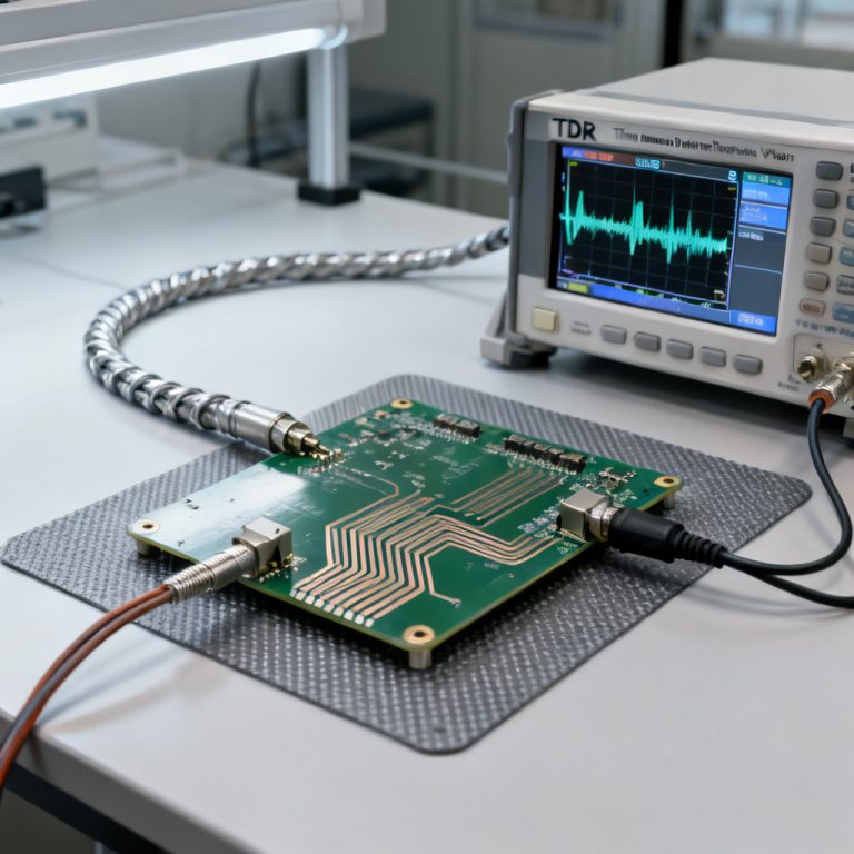
Performing a reliable TDR measurement to verify impedance control PCB accuracy requires the correct equipment and a meticulously prepared setup. This is where many errors originate.
TDR Instrument Options
- Standalone TDR: The most accurate and feature-rich option. Examples include the Tektronix 80E04 or Keysight 86100D with a TDR module. These offer the fastest rise times and advanced analysis capabilities.
- VNA (Vector Network Analyzer) with TDR Option: Many modern VNAs can perform TDR-like measurements by converting frequency-domain S-parameters to the time domain. While powerful, this method can be less intuitive for simple impedance checking and is more susceptible to calibration errors.
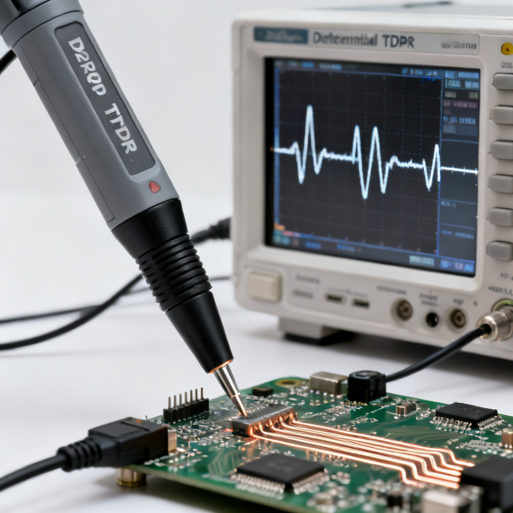
- Oscilloscope with TDR Sampling Head: A high-bandwidth sampling oscilloscope (e.g., 50 GHz) combined with a TDR sampling head is a common and highly accurate setup.
Critical Accessories and Cabling
- Low-Loss, Phase-Stable Cables: The cables from the TDR to the PCB must be of the highest quality. Any loss or impedance variation in the cable will be superimposed on your measurement.
- High-Performance Probes: For on-board measurement, you will need a probe that maintains a constant 50Ω impedance. The most common are:
- Microprobes (GS or GSG): These have a fine pitch (e.g., 500 µm, 1000 µm) and are used to contact individual traces, differential pairs, or via pads. They are the most accurate for point-to-point measurement.
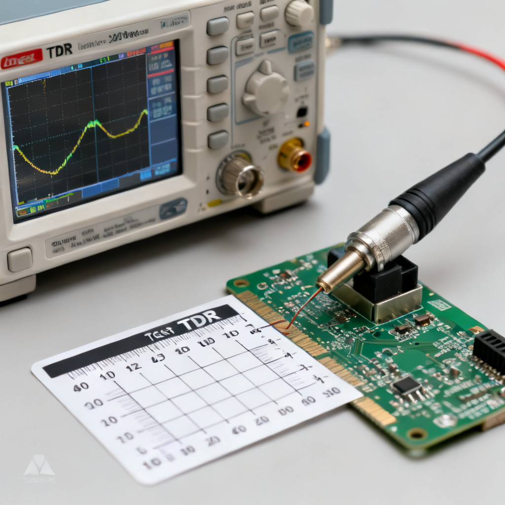
- SMA Connectors: If your PCB has dedicated SMA test points or launch connectors, this is the most repeatable method. The connector itself must be carefully designed to minimize its own impedance discontinuity.
- Calibration Standards: You must have a 50Ω load, an open, and a short. These are essential for removing the effects of your cables and probes.
The Calibration Process (The Most Critical Step)
- 1. Reference Plane: You must define your reference plane. This is the point in the measurement system where you want the TDR to consider as “perfect.” Ideally, this is at the probe tip.
- 2. Open, Short, Load (OSL) Calibration: Perform a full OSL calibration at your chosen reference plane.
- Open: Measures a perfect reflection (ρ = +1). Used to calibrate the amplitude and timing.
- Short: Measures a perfect negative reflection (ρ = -1). Used for amplitude and timing.
- Load: Measures no reflection (ρ = 0). This sets the reference impedance (e.g., 50Ω). A precision 50Ω load is the most important standard.
- 3. De-embedding: After calibration, the TDR will mathematically remove the effects of the cables and probe. This ensures that the displayed impedance is only the impedance of your PCB trace. Without proper calibration, your TDR measurement is meaningless.
Section 3: The Step-by-Step Measurement Procedure for Impedance Control PCB Accuracy
With a calibrated system, you can now proceed to measure impedance control PCB accuracy using TDR. Follow this precise protocol for repeatable, trustworthy results.
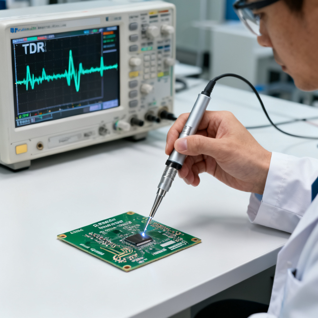
- Connect the Probe: Carefully land your microprobe on the test coupon’s launch pad or connect your SMA cable to the test connector. Ensure a solid, low-resistance contact. For differential TDR, use a differential probe (e.g., GSG) and connect both the positive and negative lines.
- Set the TDR Parameters:
- Rise Time: Select the rise time appropriate for your application. For general verification of manufacturing quality, 35-50 ps is standard. For high-precision characterization of very short stubs, use the fastest available.
- Averaging: Turn on averaging (e.g., 16x or 64x). This reduces random noise from the oscilloscope and environment, giving you a cleaner, more stable waveform.
- Time/Distance Scale: Set the horizontal scale to view the entire trace of interest. You will typically start with a wider view to see the entire coupon and then zoom in on the specific region of interest.
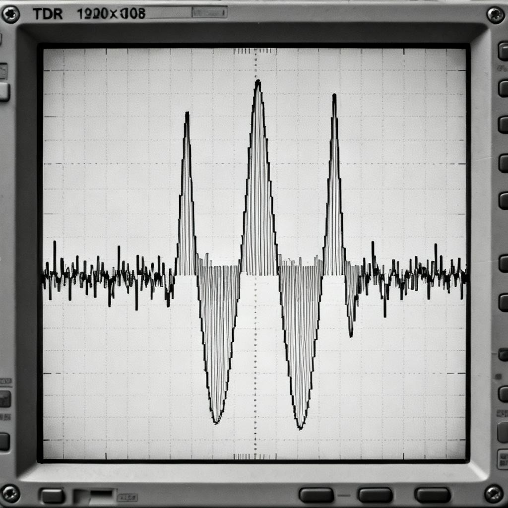
- Capture the Waveform: The TDR will display impedance (Y-axis) vs. time or distance (X-axis). You will see a trace that starts at the probe tip, jumps up to the trace impedance, and then may show features like:
- Initial Spike/Glitch: This is often the impedance of the probe-to-board transition (the launch point). It is a necessary artifact but should be minimized with good probing technique.
- Flat Region: The steady-state impedance of the trace. This is the value you are interested in.
- Ripples or Peaks: Indicate impedance variations along the trace, such as a change in dielectric thickness, a narrow neck, or a via.
- End of Trace: A sharp rise (open) or drop (short) at the end of the trace.
- Measure the Impedance:
- Average Impedance (Zavg): Most TDR instruments have a measurement cursor or a statistical function. Place two measurement gates (cursors) on the flat, steady-state region of the trace, avoiding the launch point and the end of the trace. The instrument will display the average impedance within that gate. This is the value you compare to your target impedance (e.g., 50Ω ± 10%).
- Peak Impedance: Use a single cursor to read the impedance at a specific point of interest, such as a peak or a dip. This is crucial for identifying localized defects.
- Repeat and Average: For a statistically significant result, measure multiple traces on the same board and multiple coupons across the panel. The manufacturing process has natural variation. Report the average, minimum, and maximum impedance values.
Section 4: Interpreting TDR Waveforms – A Practical Guide to Common Defects
The power of TDR lies in its ability to visualize impedance. Here is how to read the waveform to diagnose common PCB fabrication issues that affect impedance control PCB accuracy.
- Ideal Trace (Flat Line): A flat, constant impedance line at your target value (e.g., 50.2Ω). This indicates a perfectly controlled process.
- Consistent Offset (High or Low): If the flat region is consistently above or below your target, it indicates a systematic problem.
- Consistently High Impedance (e.g., 55Ω): This typically means the trace is too narrow or the dielectric is too thick. Check etching parameters or laminate thickness.
- Consistently Low Impedance (e.g., 45Ω): This indicates the trace is too wide or the dielectric is too thin. Check etching or prepreg stackup.
- Periodic Ripples (Wavy Line): A sinusoidal or wavy pattern in the impedance trace is a classic sign of glass weave effect. The trace is passing over and between the glass fiber bundles in the laminate, causing local variations in the dielectric constant (Dk). This is a fundamental material property, but it can be mitigated by using spread-glass or flat-glass laminates.
- Sharp Peak or Dip (Localized Defect):
- A sharp peak (high impedance): Could be a neck (narrowing) in the trace, an under-etched area, or a small void in the copper. It could also be a stub from a via.
- A sharp dip (low impedance): Could be a bulge in the trace (over-etching), a copper splash, or a close proximity to an adjacent ground plane.
- Gradual Slope (Impedance Gradient): A slow, linear increase or decrease in impedance along the trace. This can be caused by a gradual change in etch chemistry or a variation in laminate thickness across the panel.
- Ringing or Oscillations: High-frequency ringing after a discontinuity (e.g., a connector) indicates a parasitic inductance. This is common at via transitions and connector launches. It degrades signal integrity by causing reflections and radiated emissions.
Section 5: Advanced Considerations and Best Practices for B2B Quality
To elevate your impedance testing from a simple pass/fail check to a true quality assurance process for impedance control PCB accuracy, consider these expert-level practices.
Differential TDR (TDT)
For differential pairs (e.g., USB, HDMI, PCIe), you must measure both the differential impedance (Zdiff) and the common-mode impedance (Zcom). A single-ended TDR on one line of a pair is insufficient. You need a differential TDR instrument or a VNA with differential capability. Asymmetry in the pair (e.g., one line wider than the other) will cause mode conversion (common-mode noise), which is a major signal integrity killer.
Coupon vs. Real Trace
Always measure on a dedicated impedance test coupon located on the production panel. This coupon is designed to mimic the stackup and trace geometry of the real board. Do not try to measure a functional trace on your product board. The probe landing will damage the soldermask and copper. The coupon provides a non-destructive, representative measurement.
Temperature and Humidity Control
The dielectric constant of PCB materials is temperature and humidity dependent. For the most accurate and repeatable results, perform TDR measurements in a controlled environment (e.g., 23°C ± 2°C, 50% RH). This is especially critical for high-precision applications like RF or 100G+ designs.
Correlation with Design and Simulation
Your TDR measurement should correlate with your 2D field solver simulation (e.g., Polar Si9000, Simbeor). If the measured impedance is consistently different from your simulation, it indicates that your model’s assumptions (Dk, trace width, etch factor) are incorrect. This is a powerful feedback loop for improving your design rules.
Documentation and Reporting
A professional TDR report is a deliverable to your customer. It should include:
| Report Element | Description |
|---|---|
| Test Date and Conditions | Temperature, humidity, operator. |
| Instrument and Calibration | TDR model, rise time, calibration standards used. |
| Coupon Identification | Panel number, coupon location, trace type (e.g., single-ended, differential). |
| Measured Values | Zavg, Zmin, Zmax, and a screenshot of the TDR waveform. |
| Pass/Fail Criteria | The target impedance and tolerance (e.g., 50Ω ± 10%). |
Frequently Asked Questions About Using TDR to Measure Impedance Control PCB Accuracy
What is the best TDR rise time for measuring impedance control PCB accuracy?
The best rise time depends on the detail you need. For general verification of impedance control PCB accuracy, a rise time of 35-50 ps is standard. For high-precision characterization of very short stubs, use the fastest available rise time (e.g., 35 ps or lower).
Why is calibration critical for TDR measurement of impedance control PCB accuracy?
Calibration removes the effects of cables and probes, ensuring the displayed impedance is only from the PCB trace. Without proper calibration, your measurement of impedance control PCB accuracy will include errors from the test setup, making the results unreliable.
Can I use a VNA to measure impedance control PCB accuracy?
Yes, many modern VNAs can perform TDR-like measurements by converting frequency-domain S-parameters to the time domain. However, this method can be less intuitive for simple impedance checking and is more susceptible to calibration errors. A dedicated TDR instrument is generally preferred for direct impedance control PCB accuracy verification.
How do I interpret a wavy TDR waveform when measuring impedance control PCB accuracy?
A wavy or sinusoidal pattern in the impedance trace is a classic sign of the glass weave effect. This occurs when the trace passes over and between glass fiber bundles in the laminate, causing local variations in the dielectric constant. It can be mitigated by using spread-glass or flat-glass laminates.
What is the difference between single-ended TDR and differential TDR for impedance control PCB accuracy?
Single-ended TDR measures the impedance of one trace relative to ground. Differential TDR measures the impedance between two traces (differential impedance) and the common-mode impedance. For differential pairs (e.g., USB, HDMI, PCIe), differential TDR is essential to ensure proper impedance control PCB accuracy and avoid signal integrity issues.
“`