In high-speed PCB design, the return path—the path that current takes to return to its source—is critical for signal integrity. For rigid PCBs, designers often rely on continuous ground planes to provide a low-inductance return path. However, in flex and rigid-flex circuits, the physical structure introduces unique challenges: thin dielectrics, dynamic bending, layer transitions, and complex stack-ups. This pillar page explores the specific obstacles and provides actionable solutions to ensure robust signal integrity in flexible and rigid-flex designs.

Understanding Return Path Fundamentals in Flex Circuits
The Physics of Return Current
At high frequencies, current does not follow the path of least resistance; it follows the path of least impedance. The return current flows directly beneath the signal trace on the nearest reference plane (ground or power). For a microstrip line on a rigid board, this is straightforward. In flex circuits, the return path is often disrupted by:
- Layer discontinuities (e.g., from rigid to flex transition)
- Dynamic bending (changing capacitance and impedance)
- Thin dielectrics (increased coupling but also higher crosstalk)
- Lack of continuous ground planes in flex sections
Key Differences Between Rigid and Flex Return Paths
| Aspect | Rigid PCB | Flex/Rigid-Flex PCB |
|---|---|---|
| Reference plane | Continuous copper pour | Often segmented or absent in flex zones |
| Dielectric thickness | Controlled, uniform | Variable due to bending |
| Impedance control | Easier to maintain | Requires careful stack-up design |
| Dynamic behavior | Static | Changes with flexing |
Unique Challenges in Flex and Rigid-Flex Return Path Design
Challenge 1: Discontinuous Reference Planes at Rigid-Flex Transitions
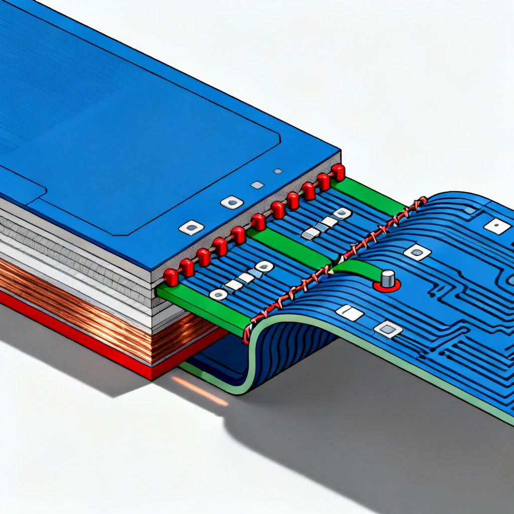
The most common issue occurs where the rigid section meets the flex section. In rigid boards, a solid ground plane is typical. In flex sections, due to mechanical flexibility requirements, ground planes may be reduced to a thin copper layer or even omitted to allow bending. This creates a return path discontinuity (RPD), leading to:
- Increased loop inductance
- Common-mode radiation
- Signal reflections
- EMI issues
Solution: Use Stitching Vias and Ground Bridges
- Place stitching vias around the transition zone to connect ground planes from rigid to flex sections.
- Use ground bridges—small copper traces or planes in the flex layer that connect to the rigid ground.
- Ensure the return path width is at least 3x the signal trace width to maintain low impedance.
Challenge 2: Dynamic Bending and Impedance Variation
When a flex circuit is bent, the dielectric thickness changes locally, altering the characteristic impedance. This is especially problematic for differential pairs (e.g., USB, HDMI) where impedance mismatch causes signal degradation.
Solution: Controlled Impedance Design with Bend Radius Consideration
- Design for a minimum bend radius (typically >10x the flex thickness) to minimize dielectric compression.
- Use impedance calculators that account for flex material properties (e.g., polyimide vs. adhesive).
- For dynamic flex, simulate the impedance variation over the bend range and adjust trace widths accordingly.
Challenge 3: Multi-Layer Stack-Up Complexity
Rigid-flex boards often combine multiple rigid layers with single or multi-layer flex sections. Each layer transition introduces a potential return path break. For example, a signal routed on a rigid layer may need to cross to a flex layer, losing its reference plane.
Solution: Layer Assignment and Return Path Planning
- Assign dedicated ground layers in both rigid and flex sections.
- Use microstrip or stripline configurations consistently. Stripline (signal between two ground planes) is preferred for high-speed signals in flex.
- Avoid routing high-speed signals across flex-to-rigid boundaries without a continuous ground reference.
Challenge 4: Thin Dielectrics and Crosstalk
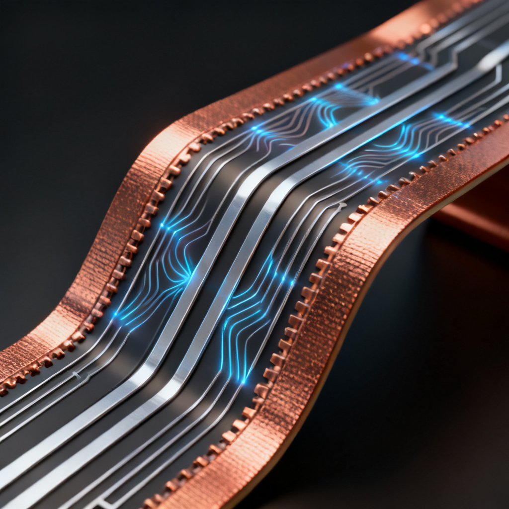
Flex materials (e.g., polyimide) are thin, leading to tight coupling between traces. While this helps with impedance control, it also increases crosstalk and common-mode noise.
Solution: Spacing and Shielding
- Increase trace-to-trace spacing in flex sections (at least 3x the dielectric thickness).
- Use grounded coplanar waveguide (GCPW) for high-speed signals in flex.
- Add ground guard traces on each side of sensitive signals.
Challenge 5: Thermal and Mechanical Stress During Assembly
Flex circuits are often subjected to reflow soldering, which can cause copper delamination or dielectric expansion, altering the return path.
Solution: Material Selection and Design Rules
- Use high-temperature polyimide (e.g., Kapton) with low CTE.
- Avoid placing vias in high-stress flex zones.
- Design with teardrops on pad-to-trace connections to reduce stress concentration.
Best Practices for Return Path Optimization in Flex/Rigid-Flex
1. Pre-Design Return Path Mapping
Before layout, create a return path map for every high-speed net. Identify where the return current will flow and ensure a continuous low-inductance path exists through all layers and transitions.
2. Use Ground Planes in Flex Sections
Even in thin flex layers, include a solid or hatched ground plane (if weight is a concern). A hatched plane (e.g., 70% copper) still provides a return path while allowing flexibility.
3. Via Placement Strategy
- Place return vias adjacent to signal vias when transitioning layers.
- For differential pairs, use via pairs with equal spacing to maintain impedance.
- In rigid-flex, use buried vias in rigid sections to avoid breaking the flex layer.
4. Simulation and Verification
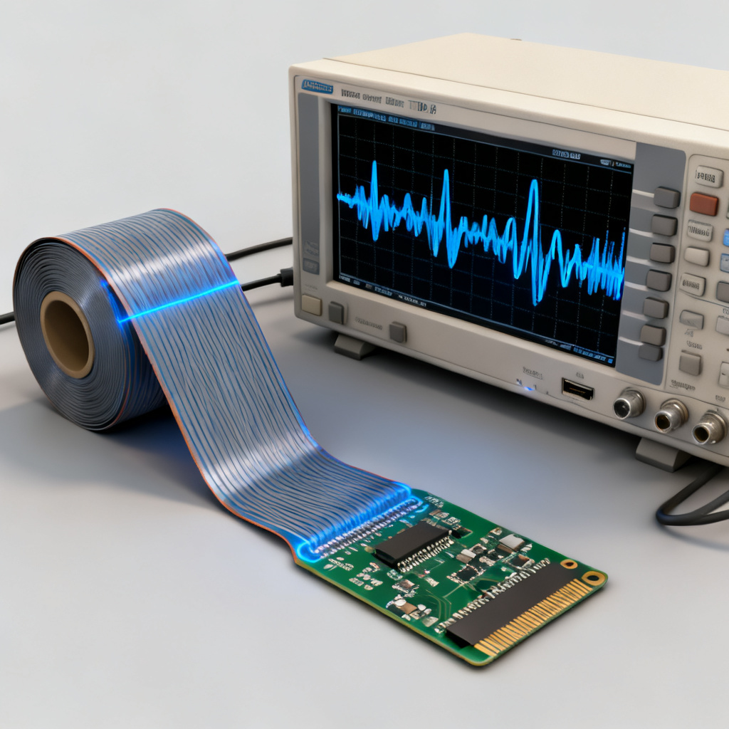
- Run 3D EM simulations (e.g., using Ansys HFSS or CST) for critical nets in flex zones.
- Perform TDR (Time Domain Reflectometry) measurements on prototypes to verify impedance and return path integrity.
5. Design for Manufacturing (DFM) Considerations
- Ensure copper balance in flex sections to prevent warping.
- Use adhesive-less laminates (e.g., Pyralux) for better thermal and electrical performance.
- Avoid 90-degree bends in traces; use 45-degree or curved routing.
Case Study: High-Speed Signal Routing in a Rigid-Flex Design
Scenario: A medical imaging device requires a rigid-flex board with a 4-layer rigid section (signal, ground, power, signal) and a 2-layer flex section (signal and ground). The design includes a 5 Gbps differential pair (USB 3.0) crossing from rigid to flex.
Problem: Initial prototype showed excessive jitter and EMI due to return path discontinuity at the transition.
Solution Applied:
- Added ground stitching vias at the rigid-flex boundary, connecting the rigid ground plane to the flex ground plane.
- Widened the flex ground trace to 15 mils (5x the signal trace width).
- Used grounded coplanar waveguide (GCPW) in the flex section with a 5 mil gap.
- Simulated the bend radius (10 mm) and adjusted impedance to 90 ohms ±10%.
Result: Jitter reduced by 40%, EMI passed FCC Class B limits.

Conclusion: Mastering Return Path for Flexible Circuits
Return path design for flex and rigid-flex PCBs is not merely an extension of rigid board practices—it requires a dedicated approach that accounts for mechanical flexibility, layer transitions, and material properties. By understanding the unique challenges (discontinuities, bending, crosstalk, and thermal stress) and applying the solutions outlined above, designers can achieve reliable high-speed performance in even the most demanding applications.
For B2B PCB manufacturers and buyers, partnering with a supplier that offers design-for-manufacturing (DFM) feedback and signal integrity simulation is essential. At [Your Company Name], we specialize in high-speed flex and rigid-flex production, ensuring your return path is optimized from prototype to volume.
Frequently Asked Questions (FAQ)
What is return path in flex PCB design?
The return path in flex PCB design refers to the route that return current takes to complete a circuit. In high-speed applications, maintaining a continuous return path is essential to minimize impedance discontinuities and signal integrity issues.
How does dynamic bending affect the return path in rigid-flex boards?
Dynamic bending changes the dielectric thickness and trace geometry, which can alter the characteristic impedance and disrupt the return path. Proper bend radius design and impedance simulation help mitigate these effects.
What are common solutions for return path discontinuity in flex circuits?
Common solutions include using stitching vias at rigid-flex transitions, adding ground bridges, and ensuring a continuous ground plane (solid or hatched) in flex sections to maintain a low-inductance return path.
Why is return path important for signal integrity in high-speed PCB design?
A poor return path increases loop inductance, causes common-mode radiation, and leads to signal reflections and EMI. For high-speed signals in flex and rigid-flex PCBs, a well-designed return path is critical for reliable performance.