For any high-speed PCB operating at 32 GT/s, the return path integrity for PCIe 5.0 is non-negotiable. This pillar page compiles the most authoritative reference plane rules from Altium, Sierra Circuits, and Cadence to ensure your design meets signal integrity requirements.
The Golden Rule: Every Signal Must Have a Continuous, Uninterrupted Reference Plane
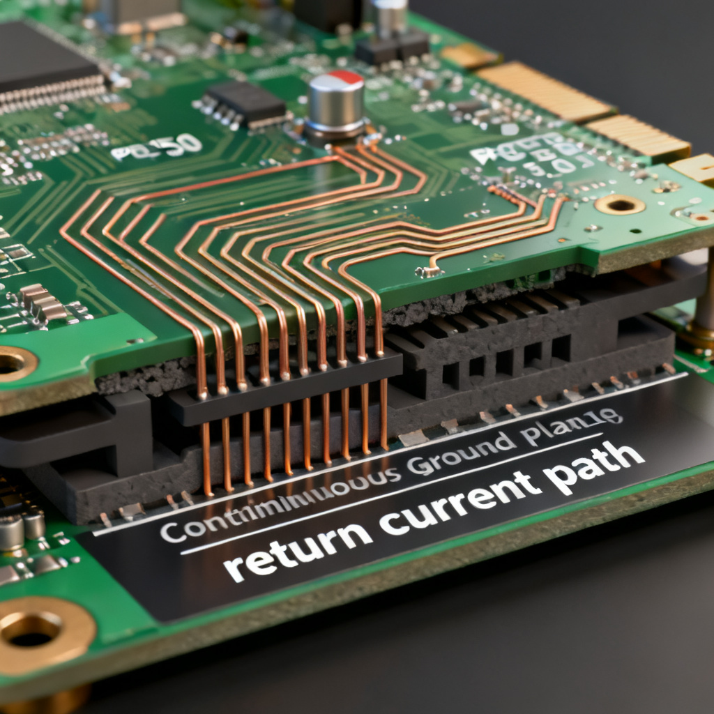
For PCIe 5.0 return path design, the most fundamental rule is that every differential pair must have a solid, continuous ground plane directly beneath it. This rule is consistently emphasized by Altium, Sierra Circuits, and Cadence.
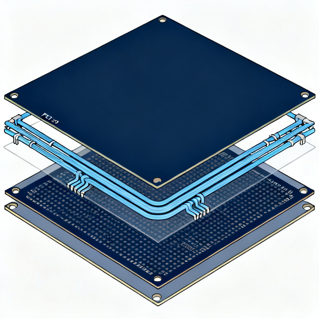
The return current for a high-speed signal flows in the plane directly adjacent to the trace due to skin and proximity effects. If the plane is split or missing, the return current must find an alternative path, creating a large loop area that radiates EMI and induces crosstalk. Never route PCIe 5.0 signals over a gap in the ground plane, such as a moat, a split between different ground regions, or a large via anti-pad. If a plane split is unavoidable, use stitching capacitors to bridge the gap.
Always Use Ground as the Reference Plane—Never Power
While a power plane can theoretically serve as a reference, for PCIe 5.0 the reference plane must be GND. Power planes have higher AC impedance due to decoupling capacitors and parasitic inductance, and they are noisier. Using a power plane as a reference introduces common-mode noise into the differential pair, degrading the eye diagram. In your stackup, place PCIe 5.0 signal layers directly adjacent to a solid GND plane, using a signal-GND-signal or GND-signal-GND configuration.
Stitching Vias and Capacitors for Plane Transitions
When a PCIe 5.0 signal must change layers, the return current must also transition. Place a ground stitching via within 30-50 mils of every signal via that transitions between layers to provide a low-inductance path. For plane splits, place a 0.1uF or 0.01uF stitching capacitor across the split, close to the crossing point, to bridge the AC return path. If a signal references a power plane and then switches to a ground plane, place a decoupling capacitor between the power and ground planes near the via—though this complex scenario should be avoided.
Maintain Consistent Reference Plane Distance (Controlled Impedance)
The distance between the trace and its reference plane determines the characteristic impedance, which should be 85Ω differential and 50Ω single-ended for PCIe 5.0. The reference plane must be uniformly spaced under the entire length of the trace. Avoid routing over large via anti-pads, thermal relief patterns, or cutouts in the ground plane. If a via is unavoidable, ensure the signal trace is at least 3x the trace width away from the anti-pad edge. Use a symmetric stackup with prepreg and core materials that maintain a consistent dielectric thickness.
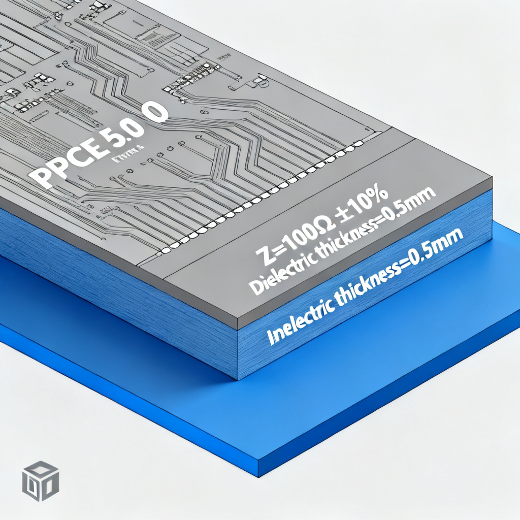
| Parameter | Target Value | Impact on Return Path |
|---|---|---|
| Differential Impedance | 85Ω ±10% | Ensures return current confinement |
| Single-Ended Impedance | 50Ω ±10% | Minimizes impedance mismatch |
| Trace Width (typical) | 5 mil | Maintains consistent plane distance |
| Trace Spacing (differential) | 8 mil | Controls coupling and return path balance |
Avoid 90-Degree Bends and Use Smooth Curves
Sharp corners create capacitive discontinuities and increase the inductance of the return path. Use 45-degree chamfered bends or curved arcs with a radius of at least 3x the trace width for PCIe 5.0 differential pairs. A 90-degree corner narrows the trace at the inside corner, increasing current density and creating a small impedance bump that degrades the return path and introduces jitter.
Minimize Layer Transitions (Keep on One Layer if Possible)
Every layer change introduces a via, which adds inductance and capacitance. Route the entire PCIe 5.0 differential pair on a single layer as much as possible. If you must change layers, do it only once near the connector or BGA. Use back-drilling to remove via stubs longer than 10 mils, as stub effects can cause resonant cavities at high frequencies.
Grounding the Connector and AC Coupling Capacitors
Connectors and AC coupling capacitors are common points of return path discontinuity. Ensure the connector has dedicated ground pins or a ground shield directly connected to the ground plane with low inductance. Place stitching vias around the connector pads to connect the top-layer ground to the inner ground plane. For AC coupling capacitors, place them directly in the signal path and keep the trace width constant under the capacitor using a dogbone pad if needed. Do not route the signal over a plane split near the capacitor.
Differential Pair Symmetry and Skew
Keep the two traces of a differential pair identical in length (skew less than 5 mils) and identical in distance to the reference plane. Any asymmetry creates common-mode current, which disrupts the return path. If you must add length to match skew, add it as a small bump or trombone near the source or destination, keeping the bump away from the connector and AC coupling caps.
Shield Critical Traces with Ground Coplanar Waveguide
For the most sensitive PCIe 5.0 signals, such as REFCLK and sideband signals, consider using a grounded coplanar waveguide structure. Place ground copper on both sides of the differential pair within 2-3x the trace width, and connect this copper to the ground plane with stitching vias every 100-200 mils. This provides a very tight return path and reduces crosstalk.
Simulation and Validation: The Final Check
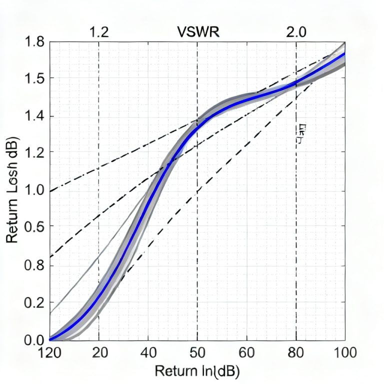
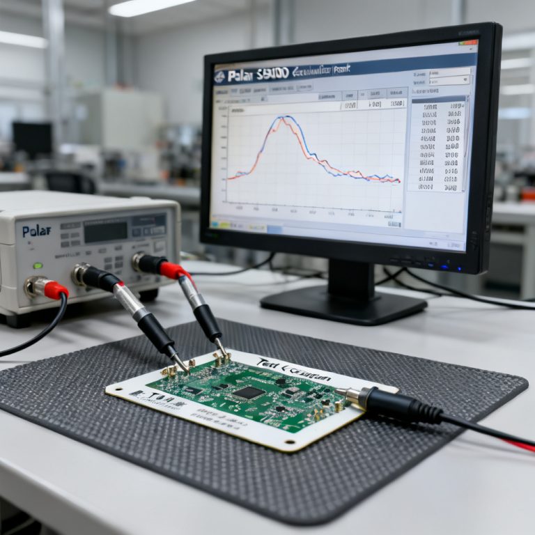
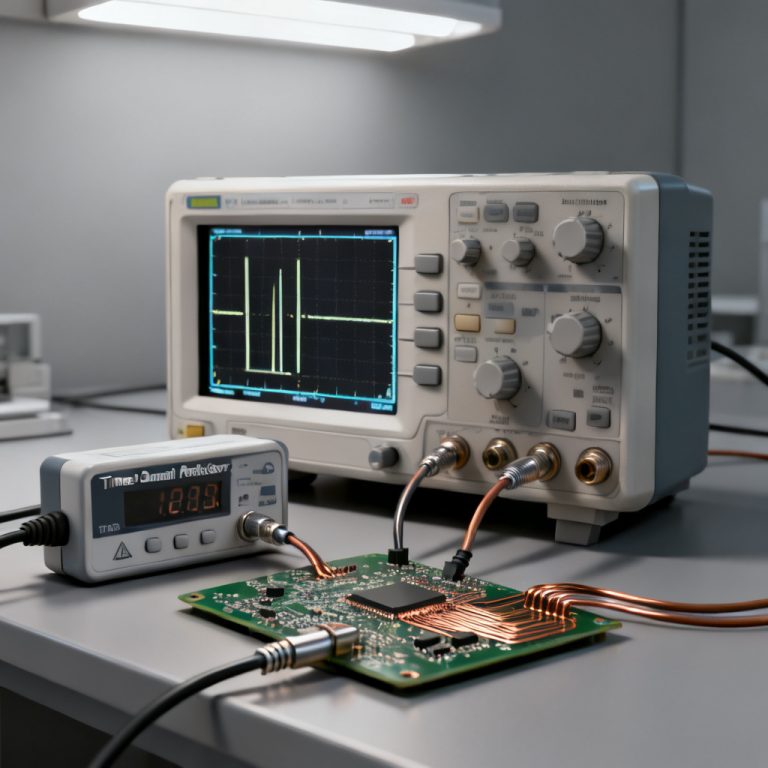
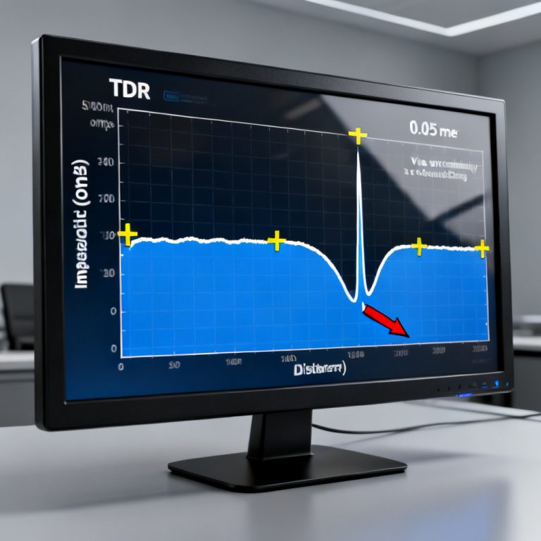
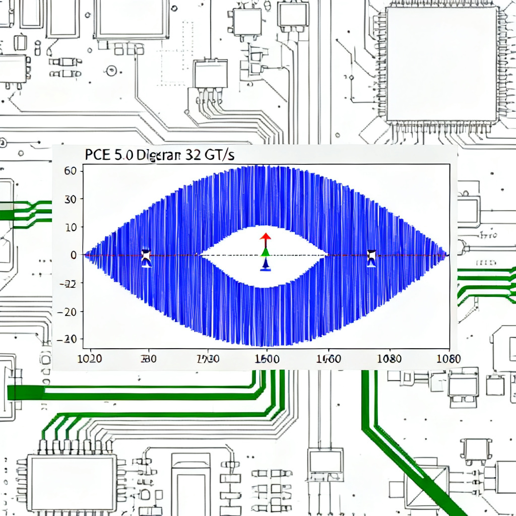
No set of rules guarantees success without simulation. Use a 3D electromagnetic solver to verify the impedance profile stays within ±10% of 85Ω differential, return loss (S11) is below -15 dB up to 16 GHz, insertion loss (S21) is flat with minimal ripple, and the eye diagram at 32 GT/s shows an opening of at least 0.5V peak-to-peak with jitter under 2 ps RMS. Physical inspection using a microscope or X-ray should check for voids, copper slivers, or via misalignment.
PCIe 5.0 Design Checklist
Before sending your PCB to manufacturing, run through this checklist:
- Reference plane: Every PCIe 5.0 trace is over a continuous GND plane.
- No plane splits: No signal crosses a gap in GND or power.
- Stitching vias: Every signal via has a GND via within 50 mils.
- Impedance: 85Ω differential, 50Ω single-ended, verified by simulation.
- Layer transitions: Minimized; back-drilled if any stubs greater than 10 mils.
- Connector grounding: Shield and ground pins are stitched to GND.
- AC coupling caps: Properly placed with no plane splits nearby.
- Skew: Less than 5 mils between traces.
- Bends: 45-degree or curved, no 90-degree.
- Simulation: Eye diagram passes at 32 GT/s.
Frequently Asked Questions
What is the return path in PCIe 5.0 PCB design?
The return path is the path taken by the current returning to its source. For PCIe 5.0, a continuous return path through a ground plane is essential to maintain signal integrity and prevent jitter.
Why must I use ground as the reference plane for PCIe 5.0?
Ground planes provide low impedance and low noise. Using a power plane introduces common-mode noise and degrades the return path, which is critical for PCIe 5.0 signal integrity.
How do stitching vias improve PCIe 5.0 return path?
Stitching vias provide a low-inductance path for return current when signals change layers, preventing loop area expansion and maintaining consistent impedance.
What is the recommended impedance for PCIe 5.0 differential pairs?
The target is 85Ω differential impedance, with a tolerance of ±10%, to ensure proper return path confinement and minimize reflections.
Can I route PCIe 5.0 over a power plane?
No. For PCIe 5.0, always use a ground plane as the reference. Power planes introduce noise and higher impedance, disrupting the return path.