In the era of AI and 112G SerDes, High Speed PCB Design is not optional—it is the foundation of reliable data transmission. Without it, modern AI infrastructure cannot function.
The convergence of artificial intelligence and 112G SerDes technology demands unprecedented signal integrity. This page explores why High Speed PCB Design matters, covering material selection, stackup, layout, and validation for 112 Gbps channels.
Why High Speed PCB Design Matters for AI and 112G SerDes
High Speed PCB Design directly impacts the performance of AI training clusters and data centers. At 112 Gbps, even minor signal degradation can halt multi-million dollar operations.

Understanding the Physics of 112G SerDes
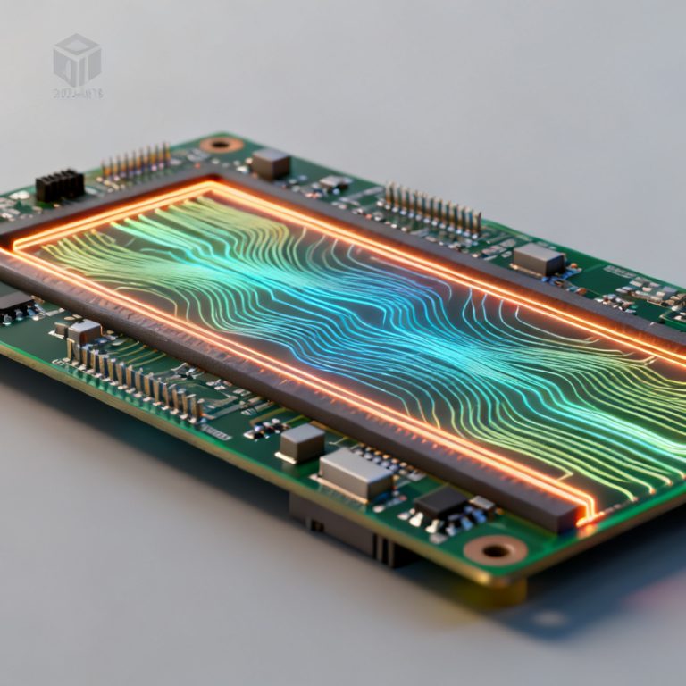
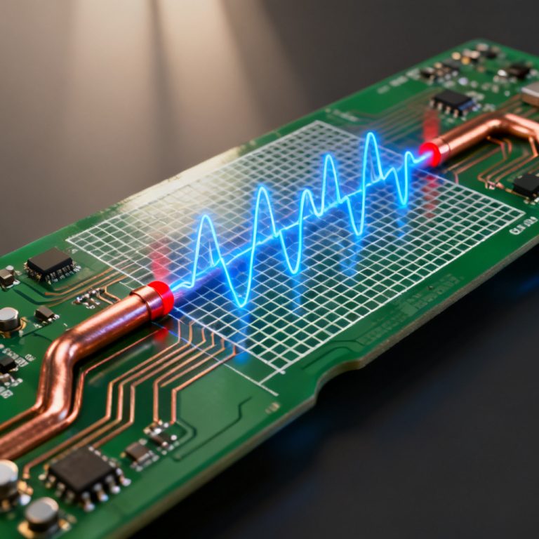
A 112G SerDes uses PAM-4 modulation, which halves the Nyquist frequency to ~28 GHz but reduces voltage margin. This makes High Speed PCB Design critical for maintaining signal integrity. Key challenges include skin effect, dielectric loss, impedance discontinuities, crosstalk, and jitter.
Signal Integrity Challenges at 112 Gbps
At 112 Gbps, insertion loss can exceed 20–30 dB over 20 inches. High Speed PCB Design must address these losses through careful material selection and layout. The small voltage margin of PAM-4 means any degradation directly affects bit error rates.
| Parameter | Impact on High Speed PCB Design | Requirement for 112G |
|---|---|---|
| Skin Effect | Increases AC resistance at high frequencies | Use smooth copper foil (VLP/HVLP) |
| Dielectric Loss (Df) | Absorbs signal energy | Df ≤ 0.003 at 10 GHz |
| Impedance Discontinuity | Causes reflections | Impedance tolerance ±5% |
| Crosstalk | Reduces voltage margin | Guard traces and spacing |
| Jitter | Timing errors | Total jitter < 0.1 UI |
Each of these challenges is magnified in High Speed PCB Design for AI workloads. The physics of 112G SerDes demands rigorous engineering.
Material Selection for High Speed PCB Design
Material selection is the most impactful decision in High Speed PCB Design for 112G SerDes. Standard FR-4 is unusable due to high dielectric loss and CTE mismatch.
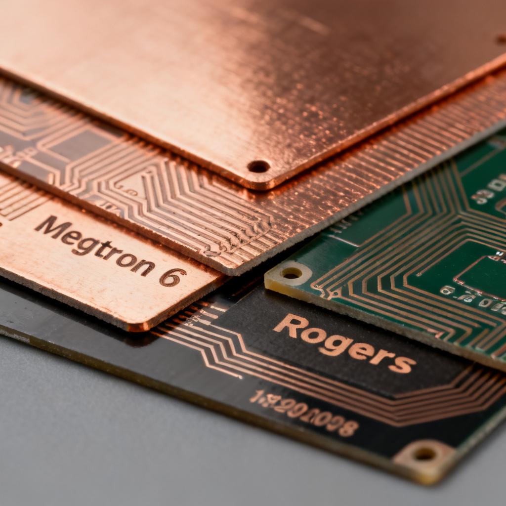
Low-Loss Materials Required for 112G
For High Speed PCB Design, ultra-low-loss materials like MEGTRON 6 (Df ~0.002), Rogers 3000 series (Df ~0.0013), and Isola I-Tera MT40 are mandatory. These materials ensure signal integrity at 28 GHz+.
Copper Foil Roughness and Its Impact
In High Speed PCB Design, copper foil roughness significantly affects conductor loss. VLP or HVLP copper foil is required for 112G SerDes channels. The smoother the foil, the lower the loss.
Hybrid Stackups for Cost Optimization
A common strategy in High Speed PCB Design is using hybrid stackups: low-loss materials for signal layers and standard FR-4 for power/ground. This balances performance and cost.
| Material | Df at 10 GHz | Application in High Speed PCB Design |
|---|---|---|
| MEGTRON 6 | ~0.002 | Backplanes, high-layer-count boards |
| Rogers RO3003 | ~0.0013 | RF and millimeter-wave |
| Isola I-Tera MT40 | ~0.004 | Thermal reliability |
| Nelco N4000-13SI | ~0.008 | Cost-sensitive designs |
Choosing the right material is the first step in successful High Speed PCB Design for AI and 112G SerDes.
Stackup Design for High Speed PCB Design
Stackup design is the blueprint for High Speed PCB Design. A poor stackup will compromise even the best materials.
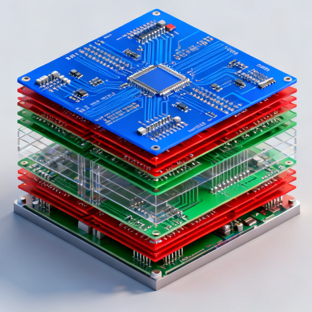
Symmetry and Balanced Construction
In High Speed PCB Design, a symmetrical stackup prevents warpage. For a 20-layer board, layers 1 and 20 should have similar copper weight and prepreg type.
Signal-to-Reference Plane Proximity
Every high-speed trace must be adjacent to a solid reference plane. In High Speed PCB Design, the dielectric thickness is typically 3–4 mils for 50-ohm impedance.
Via Stub Management
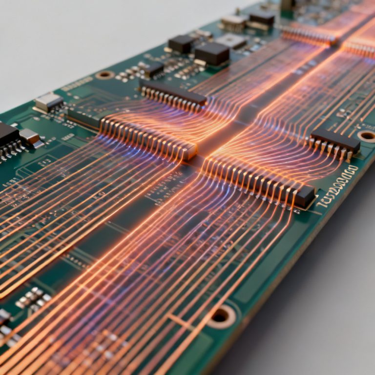
Via stubs create resonant nulls at 112G. High Speed PCB Design requires back-drilling with ±2 mil tolerance. Micro-vias or buried vias eliminate stubs entirely.
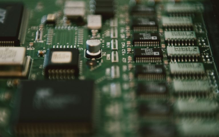
Layout and Routing for High Speed PCB Design
Layout execution determines whether High Speed PCB Design succeeds or fails. Poor routing will destroy signal integrity.
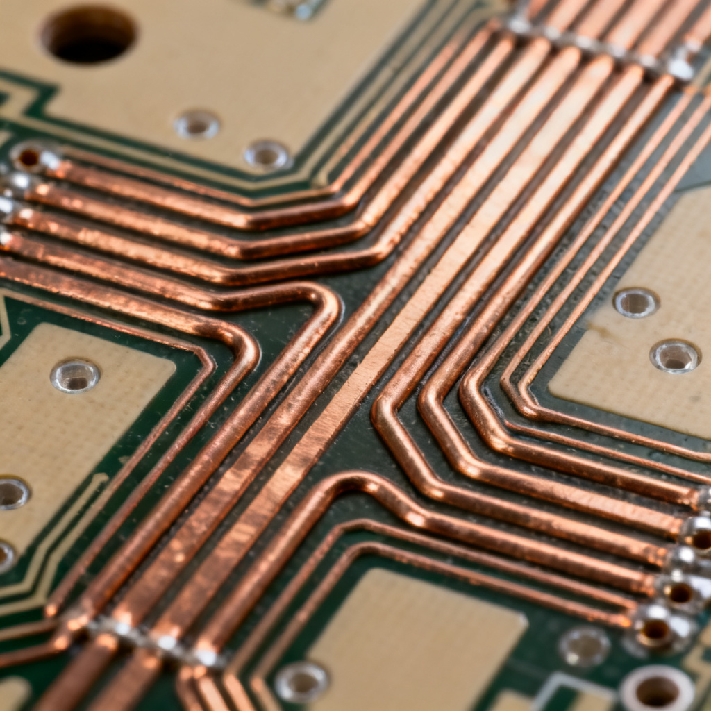
Trace Geometry and Length Matching
In High Speed PCB Design, trace width is calculated for 50 ohms. Differential pairs must be length-matched to ±2 mils. Use 45-degree chamfers or curved arcs.
Component Placement for 112G SerDes
Place SerDes transceivers as close to connectors as possible. AC coupling capacitors must be on the same layer with no vias between them and the transceiver.
Power Integrity for SerDes
High Speed PCB Design must address power integrity. Use decoupling capacitors with PDN impedance < 1 mΩ up to 1 GHz for 112G SerDes.
Simulation, Testing, and Validation
Simulation is mandatory in High Speed PCB Design for 112G SerDes. Without it, design failures are inevitable.

Pre-Layout and Post-Layout Simulation
Use 3D EM solvers to model S-parameters and TDR impedance. In High Speed PCB Design, post-layout eye diagram simulation must show a clear, open eye.
Testing and Validation
Test with TDR, VNA (up to 40 GHz), and BERT. A passing channel in High Speed PCB Design must have BER < 1e-15.
High Speed PCB Design vs. Conventional Design
Compared to conventional PCB design, High Speed PCB Design for 112G SerDes requires stricter tolerances, advanced materials, and rigorous simulation. Standard FR-4 and 90-degree corners are unacceptable. Our expertise in High Speed PCB Design ensures reliable performance for AI workloads.
Frequently Asked Questions about High Speed PCB Design
What is High Speed PCB Design?
High Speed PCB Design refers to the engineering discipline of designing printed circuit boards for signals above 1 GHz, addressing signal integrity, impedance control, and material selection. For 112G SerDes, it is essential.
Why is High Speed PCB Design important for AI?
AI training clusters rely on High Speed PCB Design to ensure reliable data transmission at 112 Gbps. Poor design leads to errors, latency, and costly failures.
What materials are used in High Speed PCB Design for 112G?
Ultra-low-loss materials like MEGTRON 6 and Rogers 3000 series are standard in High Speed PCB Design for 112G SerDes. Standard FR-4 is not suitable.
How does High Speed PCB Design handle signal integrity?
High Speed PCB Design addresses signal integrity through impedance control, back-drilling, low-loss materials, and simulation. These techniques ensure reliable 112G channels.
“`