In high-speed PCB design, understanding how switching reference planes affects return path PCB design (VCC vs GND) is critical for maintaining signal integrity. When a signal trace changes layers, the return current must follow a low-inductance path to avoid impedance discontinuities and electromagnetic interference. This guide synthesizes expert insights to help you master plane transitions.
Fundamental Physics of Return Path in High-Speed PCB Design
The return path in high-speed PCB design is governed by the path of least inductance, not resistance. At high frequencies above 1 MHz, return current concentrates directly under the signal trace within a distance equal to the dielectric height multiplied by 3 to 5. This minimizes loop inductance and ensures signal integrity. Any disruption to this loop, such as switching reference planes, increases the loop area and degrades performance.
Key Principles from Top Sources
High-Frequency Behavior: At DC or low frequencies, return current spreads across the entire plane. At high frequencies, it stays close to the signal trace. The Loop Area Rule: Smaller loop area reduces inductance and EMI. Reference Plane Role: Both GND and VCC planes serve as AC grounds, but they are not identical. GND provides a universal, stable 0V reference, while VCC carries power supply noise.
Critical Distinction: VCC vs GND as Reference Planes in Return Path PCB Design
Switching reference planes between VCC and GND introduces impedance discontinuities. GND is the ideal reference plane due to its low impedance and noise immunity. VCC, while acting as an AC ground at high frequencies, is often segmented and noisy. When a signal transitions from a GND-referenced layer to a VCC-referenced layer, the return current must jump planes, creating a large loop if not properly managed.
GND as the Ideal Reference Plane
Universality: GND provides a global 0V reference for all signals. Low Impedance: A solid GND plane offers the lowest impedance for return currents. Noise Immunity: GND planes are quiet, making them preferred for critical high-speed signals like clocks and serial data lines.
VCC as a Reference Plane – The “AC Ground” Trap
AC Ground Behavior: At high frequencies, VCC is an AC ground through decoupling capacitors, but only if the VCC plane is continuous. The Problem: VCC planes are often segmented into different voltage domains, causing return path disruptions. Additionally, VCC carries power supply noise that can couple into signals. The Critical Rule: Never route a high-speed signal over a split in its reference plane. Splits in VCC are more common than in GND.
The Impedance Discontinuity
When switching from GND to VCC, the return current must jump from the GND plane to the VCC plane. Without a low-inductance path, the return current flows around the via or through a distant decoupling capacitor, creating a large loop and a significant impedance spike from 50Ω to 80Ω or higher.
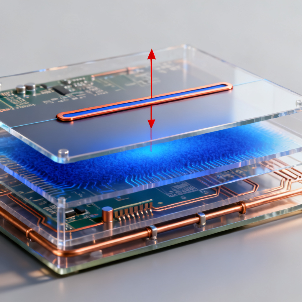
Via Stitching and Return Via Placement for Plane Transitions
All authoritative sources converge on the solution: provide a direct, low-inductance path for the return current at the point of the plane transition. This is achieved through return vias, also called stitching vias or ground vias.

What is a Return Via?
A return via connects the two reference planes, such as GND and VCC, as close as possible to the signal via. This allows the return current to jump from one plane to the other immediately, maintaining a small loop area. Distance Rule: Place the return via within 1/10th of the signal’s rise time wavelength, typically 1-2 mm for a 1 GHz signal. For very high-speed signals above 10 Gbps, use two or three return vias around the signal via to reduce inductance.
Why a Single Via is Not Enough
A single signal via without a return via creates a via stub effect and a large loop. The return current must travel to the nearest decoupling capacitor, which may be inches away, introducing delay and resonance. A dedicated return via provides a path right at the transition point.
The VCC-GND Stitching Strategy
For GND to VCC transitions, place a GND via near the signal via. For VCC to GND transitions, the same principle applies. In a standard 4-layer stackup with Signal-GND-VCC-Signal, when a signal switches from top to bottom, you need a return via from the GND plane to the VCC plane, often a GND via connecting both planes.
Practical Design Rules for Switching Reference Planes
Based on authoritative sources, here are actionable design rules for high-speed PCB layout.
Rule 1: Prefer GND as the Primary Reference
Route all critical high-speed signals on layers adjacent to a solid GND plane. Use a stackup like GND-Signal-Signal-GND for stripline or Signal-GND-VCC-Signal for microstrip/stripline hybrid. Ensure every signal layer is directly adjacent to a GND plane.
Rule 2: Avoid Splits in the Reference Plane
Never route a signal over a split in its reference plane. If you must cross a split for a voltage island, use a stitching capacitor, such as 100 nF, across the split placed as close to the crossing point as possible.
Rule 3: Place Return Vias Immediately Adjacent to Signal Vias
Every signal via that changes reference plane must have a return via. The return via should be no further than 1.5 mm from the signal via for signals with rise times under 1 ns. For differential pairs, place a return via for each signal via or one return via between the two signal vias.
Rule 4: Use Multiple Vias for High-Frequency Transitions
For signals above 5 GHz, use a cluster of 2-3 return vias around the signal via to reduce effective inductance.
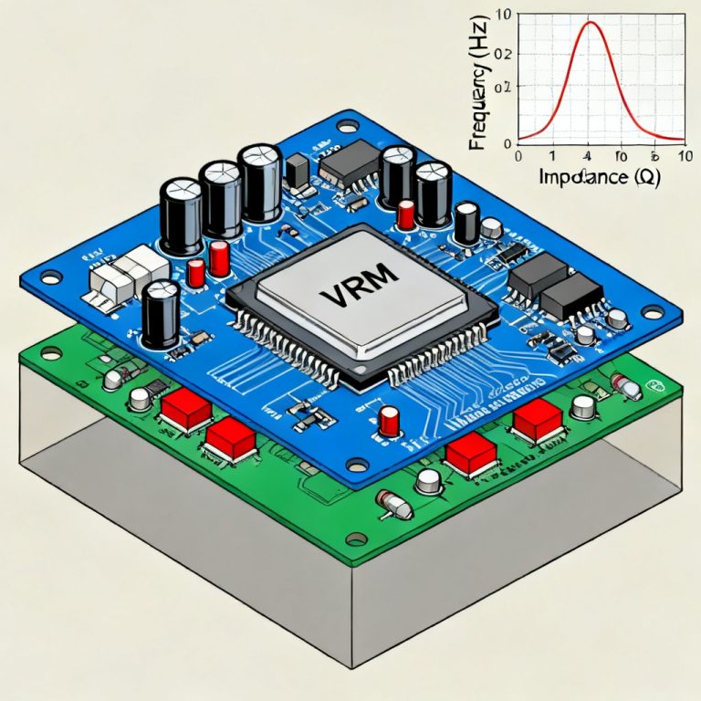
Rule 5: Model and Simulate the Transition
Use a 3D field solver like Ansys HFSS or CST to analyze the impedance of the via transition. Target impedance matching within 50Ω ± 10%.
Common Mistakes in Return Path PCB Design and How to Avoid Them
| Mistake | Consequence | Solution |
|---|---|---|
| No return via | Large loop area, high EMI, signal reflection | Always add a return via within 1/10 of signal rise time |
| Return via too far | Return current takes longer path, creating stub | Keep distance under 1.5 mm for high-speed signals |
| Routing over VCC split | Severe impedance discontinuity, signal loss | Route over continuous GND; if VCC is reference, ensure solid plane |
| Using single VCC plane | Noise coupling from power supply into signal | Use dedicated GND planes for critical signals |
| Ignoring via anti-pads | Large anti-pads create capacitive discontinuity | Use small anti-pads, e.g., 10 mils larger than via pad |
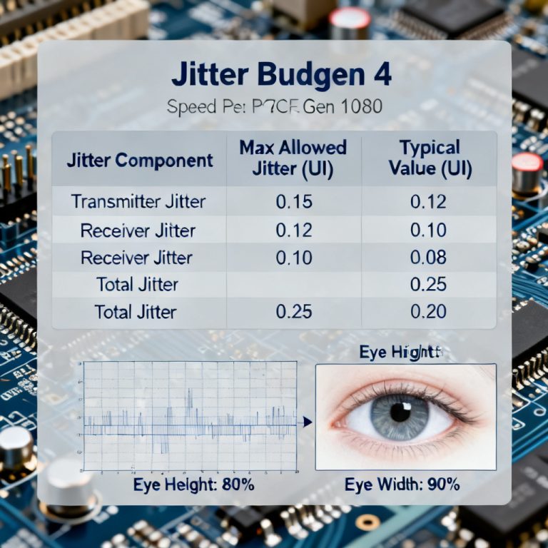
Case Study: 10 Gbps SerDes Transition in High-Speed PCB
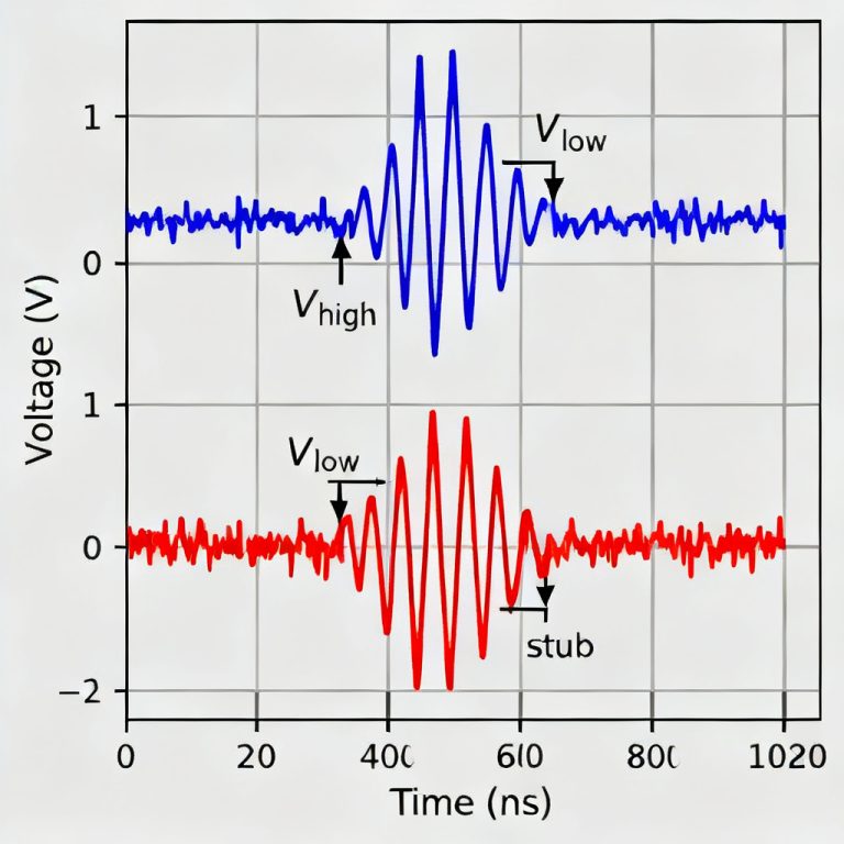
Consider a 10 Gbps SerDes signal transitioning from a top-layer microstrip referenced to GND to a bottom-layer stripline referenced to VCC. Without proper design, the return current must travel to the nearest GND-to-VCC decoupling capacitor 300 mils away, creating a 40-ohm impedance dip and 3 dB insertion loss at 5 GHz. With a GND via placed 1 mm from the signal via, the return current jumps instantly from GND to VCC, maintaining 50-ohm impedance and an open eye diagram with minimal jitter. This demonstrates that a well-designed via transition is as critical as trace impedance itself.
Frequently Asked Questions About Switching Reference Planes
What is the return path in high-speed PCB design?
The return path in high-speed PCB design is the path taken by return current, which at high frequencies follows the path of least inductance directly under the signal trace to minimize loop area and maintain signal integrity.
How does switching reference planes affect return path PCB design?
Switching reference planes, such as from GND to VCC, disrupts the return path by forcing the return current to jump between planes. Without proper via stitching, this creates a large loop area, impedance discontinuity, and increased EMI.
What is the difference between VCC and GND reference planes?
GND is a universal, low-impedance, noise-free reference plane ideal for high-speed signals. VCC acts as an AC ground at high frequencies but is often segmented and noisy, making it less suitable for critical signals unless properly managed with stitching vias.
What is a return via in PCB design?
A return via, also called a stitching via, is a via placed near a signal via to provide a low-inductance path for the return current when switching reference planes, ensuring a small loop area and maintaining impedance control.
How do I design for plane transitions in high-speed PCBs?
To design for plane transitions, prefer GND as the primary reference, avoid splits in reference planes, place return vias within 1.5 mm of signal vias, use multiple vias for high-frequency signals, and simulate transitions with field solvers.