In modern high-speed digital systems, SSO noise (Simultaneous Switching Output) is a critical factor that directly degrades power integrity PCB performance. As data rates climb and supply voltages drop, even minor noise on power distribution networks (PDN) can cause logic errors, signal jitter, and system failures. This pillar page consolidates the most authoritative knowledge from leading industry sources, providing a deep dive into SSO noise mechanics, its detrimental effects on power integrity, and actionable design solutions for robust PCB layouts.
Understanding SSO Noise – The Root Cause of Power Integrity PCB Issues
What is SSO Noise?
SSO noise, often referred to as simultaneous switching noise (SSN) or ground bounce, occurs when multiple output buffers switch states (e.g., from logic 0 to 1 or 1 to 0) at the same time. This rapid current draw through the shared power and ground paths induces voltage transients across parasitic inductances in the PDN. According to leading technical sources, the key drivers are:
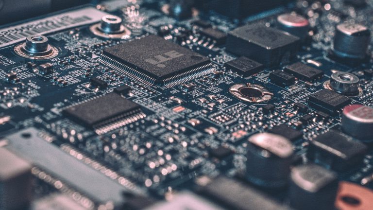
- Package and bond wire inductance: In IC packages, bond wires and lead frames have inherent inductance (typically 1-10 nH per pin). When many outputs switch simultaneously, the total di/dt through these inductances generates a voltage spike: V = L × (di/dt).
- PCB trace and via inductance: The power and ground planes, as well as vias connecting them, contribute additional inductance.
- On-chip decoupling limitations: Internal decoupling capacitors have finite bandwidth and cannot supply instantaneous current for high-speed switching events.
The Physics Behind Ground Bounce
When outputs switch from high to low, current flows from the load capacitance through the output driver to ground. The return current through the ground inductance creates a voltage rise at the chip’s internal ground relative to the board ground. This is ground bounce. Conversely, switching from low to high causes a drop in the internal VDD rail (power supply droop). Both effects are manifestations of SSO noise.
Key parameters influencing noise magnitude:
- Number of simultaneously switching outputs (N): Noise scales linearly with N.
- Switching speed (slew rate): Faster edges increase di/dt.
- Output capacitance load: Larger loads require more charge, increasing peak current.
- Inductance of the PDN path: Lower inductance reduces noise amplitude.
Impact of SSO Noise on Power Integrity PCB
Degradation of Voltage Margins
Power integrity demands that the supply voltage at the IC remain within specified tolerances (e.g., ±5% for 1.8V logic). SSO noise causes:
- Power supply droop: A temporary drop in VDD due to high current demand, potentially causing logic ‘1’ levels to fall below the input threshold.
- Ground bounce: A rise in internal ground potential, which can make a logic ‘0’ appear as a ‘1’ to the receiving gate.
These violations lead to timing errors, data corruption, and reduced noise margins.
Induced Jitter and Timing Failures
SSO noise directly translates into timing uncertainty:
- Voltage-dependent delay: The propagation delay of CMOS gates varies with supply voltage. A drooping VDD increases gate delay, causing output signals to arrive later than expected.
- Ground bounce induced skew: Different outputs may experience different ground bounce levels, creating skew between signals that should be synchronized.
This jitter is particularly problematic for high-speed interfaces like DDR memory, PCIe, and SerDes, where setup/hold times are tight.
Impact on Signal Integrity (SI)
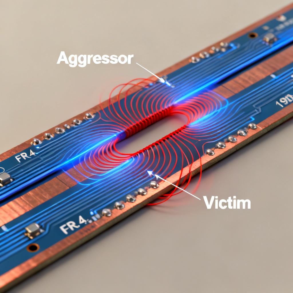
SSO noise couples into signal paths through:
- Simultaneous switching output (SSO) crosstalk: The noise on the PDN modulates the output voltage of quiet drivers, creating false transitions or glitches.
- Return current disruption: Ground bounce forces return currents to flow through unintended paths, increasing loop inductance and radiated emissions.
This degrades eye diagrams, increases bit error rates (BER), and can cause electromagnetic interference (EMI) failures.
Long-Term Reliability Concerns
Repeated SSO events stress the IC’s internal power grid and decoupling capacitors. Over time, this can lead to:
- Electromigration in power traces.
- Accelerated aging of on-chip decoupling capacitors.
- Thermal hotspots due to concentrated current flow.
These effects reduce product lifespan, especially in high-reliability applications like automotive or aerospace.
Quantifying SSO Noise – Key Metrics and Simulation for Power Integrity PCB
PDN Impedance Target
A critical metric for power integrity is the target impedance (Ztarget) of the PDN: Ztarget = (VDD × ripple tolerance) / ΔI, where ΔI is the transient current demand. For SSO noise, the PDN must maintain low impedance from DC up to the maximum switching frequency (e.g., 1 GHz for 2 Gbps data rates). Exceeding this impedance causes excessive voltage noise.
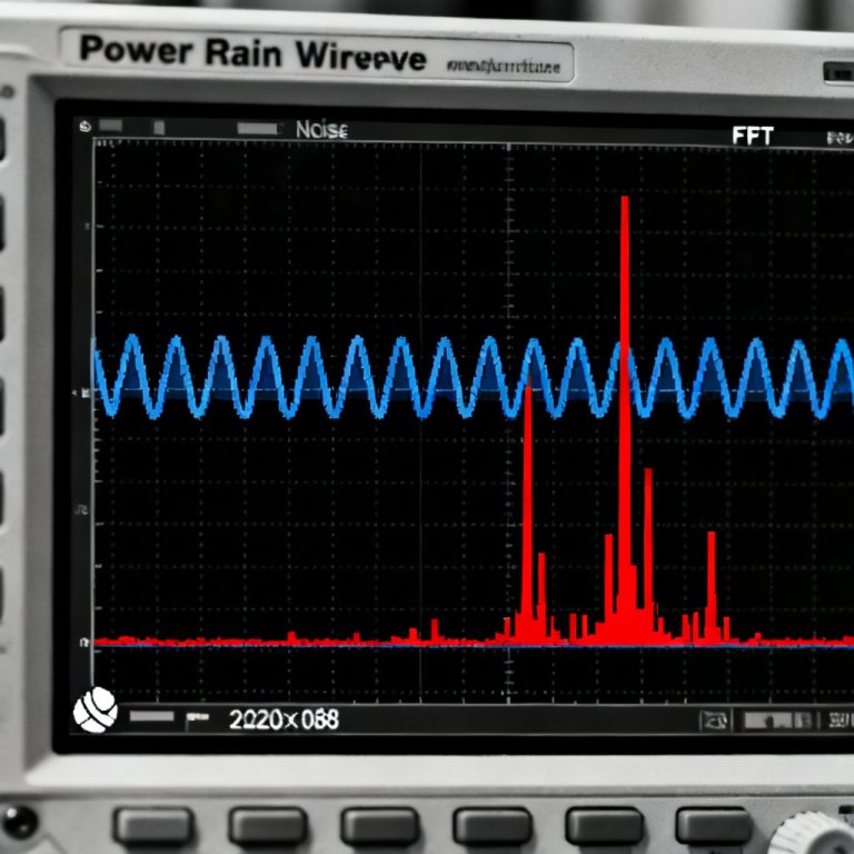
Time-Domain vs. Frequency-Domain Analysis
- Time-domain simulation: Using tools like SPICE or IBIS models, engineers can simulate the exact voltage waveforms at the IC’s power pins during a switching event. This reveals peak noise amplitude, duration, and ringing.
- Frequency-domain analysis: S-parameter measurements or simulations of the PDN (including PCB, package, and on-chip decoupling) show impedance vs. frequency. Peaks in impedance correspond to resonant frequencies where SSO noise is amplified.
Industry-Standard Models
- IBIS (I/O Buffer Information Specification): Provides accurate I/O switching currents and package parasitics for SSO noise simulation.
- Power-aware IBIS (IBIS 6.0+): Includes power integrity data for simultaneous switching analysis.
- 3D EM simulation: Tools like Ansys HFSS or CST model the PCB’s PDN as a distributed network, capturing plane resonances and via inductance.
Mitigation Strategies – Designing for Low SSO Noise in Power Integrity PCB
Optimizing the Power Distribution Network (PDN)
- Use solid power and ground planes: Dedicated planes minimize loop inductance. Avoid splits or slots under high-speed I/O areas.
- Minimize via inductance: Use multiple vias in parallel for power connections, and place them as close as possible to the IC’s power pins.
- Increase plane capacitance: Thin dielectric layers (e.g., 100 μm) between power and ground planes create high-frequency decoupling capacitance.
- Select low-inductance packages: BGA or QFN packages with short bond wires and multiple power/ground pins outperform leaded packages.
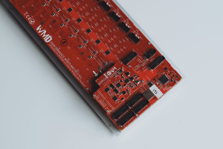
Strategic Decoupling Capacitor Placement
- Use a multi-tier decoupling strategy:
- Bulk capacitors (10-100 μF): Located near the power entry point, supply low-frequency current.
- Mid-frequency capacitors (0.1-1 μF): Placed around the IC, suppress mid-band PDN impedance peaks.
- High-frequency capacitors (10-100 nF): Positioned directly under or adjacent to the IC’s power pins, handle the fastest current transients.
- Minimize capacitor ESL: Use 0402 or 0201 packages with low equivalent series inductance (ESL). Connect capacitors with short, wide traces to vias.
- Use embedded capacitance: For extreme high-speed designs, embed thin dielectric layers within the PCB to create distributed decoupling capacitance (e.g., 100-500 pF/in²).
I/O Buffer and Circuit Techniques
- Reduce slew rate: Use output drivers with controlled edge rates (e.g., 0.5-1 V/ns) to lower di/dt, at the cost of increased timing jitter.
- Implement staggered switching: In multi-bit buses, delay the switching of individual outputs by a few picoseconds to spread the current demand.
- Use differential signaling: For critical high-speed interfaces (e.g., LVDS, CML), differential signals inherently cancel SSO noise because the current draw is balanced.
- Add on-chip decoupling: Modern ICs integrate deep trench or MIM capacitors that provide fast local charge storage.
PCB Layout Best Practices
- Route power and ground as a transmission line: Keep power traces wide and short, with a continuous ground return path.
- Avoid long daisy chains: Connect each IC directly to the power plane with a dedicated via, not through a shared trace.
- Use ground vias for signal transitions: When a signal changes layers, place a ground via nearby to provide a low-inductance return path.
- Maintain consistent stackup: Use a symmetric stackup with power and ground planes adjacent to signal layers to minimize loop area.
Case Studies and Real-World Examples of SSO Noise in Power Integrity PCB
DDR Memory Interface Failure
A common scenario: A 32-bit DDR3 bus operating at 1600 MT/s experiences intermittent data errors. Analysis reveals:
- SSO noise of 250 mV on the VDD rail during simultaneous write operations.
- Ground bounce of 180 mV, causing a false read of a logic ‘0’.
Solution: Adding 100 nF decoupling capacitors in 0402 package directly under the memory controller, plus increasing the number of ground vias from 4 to 12, reduced noise to 80 mV.
FPGA-Based High-Speed Serial Link
A Xilinx Kintex-7 FPGA with 16 GTY transceivers shows excessive jitter (15 ps RMS) on the output clock.
Root cause: SSO noise from 48 simultaneous LVCMOS I/Os switching at 200 MHz, coupled into the transceiver’s PLL power supply.
Fix: Isolating the transceiver power domain with a ferrite bead and dedicated decoupling, plus reducing the slew rate of the LVCMOS outputs, lowered jitter to 3 ps RMS.
Measuring and Validating SSO Noise for Power Integrity PCB
On-Board Measurement Techniques
- Use a high-bandwidth oscilloscope (≥ 4 GHz) with low-inductance probes: Solder a 50-ohm coaxial probe directly to the IC’s power and ground pins, avoiding long ground leads.
- Measure at the IC’s power ball: Use a micro-probe or a test via placed within 2 mm of the IC’s power pin.
- Trigger on the switching event: Use a clock or strobe signal to capture the noise transient.
Interpreting Measurement Results
- Peak-to-peak noise: Compare against the IC’s specified tolerance (e.g., ≤ 100 mV for 1.2V logic).
- Ringing frequency: Identify PDN resonances (e.g., 200 MHz ringing indicates a plane resonance).
- Rise time of noise: Faster rise times (e.g., < 1 ns) indicate that decoupling is insufficient at high frequencies.
Correlation with Simulation
- Use S-parameter measurements of the actual PCB to validate the simulated PDN impedance.
- Adjust IBIS model parameters (e.g., package inductance) to match measured noise waveforms.
- Iterate on decoupling placement until measured noise falls below the target.
Comparison of SSO Noise Mitigation Techniques for Power Integrity PCB
| Technique | Effectiveness for SSO Noise | Implementation Complexity | Typical Noise Reduction |
|---|---|---|---|
| Solid power/ground planes | High | Low | 30–50% |
| Multi-tier decoupling capacitors | High | Medium | 40–60% |
| Reduced slew rate | Medium | Low | 20–40% |
| Staggered switching | Medium | Medium | 15–30% |
| Differential signaling | Very High | High | 60–80% |
Glossary of Key Terms in SSO Noise and Power Integrity PCB
- SSO noise (Simultaneous Switching Output noise): Voltage transients induced on the power distribution network when multiple output drivers switch simultaneously.
- Ground bounce: A rise in the internal ground potential of an IC due to current flow through ground inductance during switching.
- Power supply droop: A temporary drop in supply voltage caused by high transient current demand.
- PDN impedance: The impedance of the power distribution network as a function of frequency; low impedance is critical for power integrity.
- Decoupling capacitor: A capacitor placed near an IC to supply instantaneous current and reduce noise on the power rail.
- di/dt: The rate of change of current over time; a key factor in generating SSO noise.
Frequently Asked Questions about SSO Noise and Power Integrity PCB
What is SSO noise in power integrity PCB design?
SSO noise (Simultaneous Switching Output noise) is a voltage transient on the power distribution network caused by multiple output buffers switching at the same time. It directly impacts power integrity PCB performance by causing ground bounce and power supply droop.
How does SSO noise affect signal integrity in high-speed PCBs?
SSO noise induces jitter and timing skew, degrades eye diagrams, and increases bit error rates. In power integrity PCB design, it couples into signal paths through crosstalk and return current disruption, compromising overall system reliability.
What are the best mitigation strategies for SSO noise in power integrity PCB?
Key strategies include using solid power/ground planes, strategic decoupling capacitor placement, reducing output slew rates, implementing staggered switching, and using differential signaling. These techniques significantly reduce SSO noise and improve power integrity PCB performance.
How do I measure SSO noise on a power integrity PCB?
Use a high-bandwidth oscilloscope (≥ 4 GHz) with low-inductance probes soldered directly to the IC’s power and ground pins. Measure peak-to-peak noise, ringing frequency, and rise time to assess SSO noise impact on power integrity.
Conclusion: Mastering SSO Noise for Reliable Power Integrity PCB
SSO noise is a pervasive challenge in high-speed PCB design, directly undermining power integrity and system reliability. By understanding its root causes—parasitic inductance, high di/dt, and limited decoupling—engineers can implement targeted mitigation strategies: robust PDN design, strategic decoupling, controlled slew rates, and careful layout. The industry’s best practices, validated through simulation and measurement, ensure that even the most demanding digital systems operate with clean power and minimal jitter.
For B2B PCB manufacturers and designers, mastering SSO noise is not optional—it is a competitive differentiator. By integrating these techniques into your design flow, you deliver high-speed PCBs that meet the stringent performance requirements of modern electronics.
Call to Action: Need a high-speed PCB with optimized power integrity? Contact our engineering team for a free SSO noise analysis and design review. We specialize in multi-layer PCBs for DDR, PCIe, and SerDes applications—built to your exact specifications.