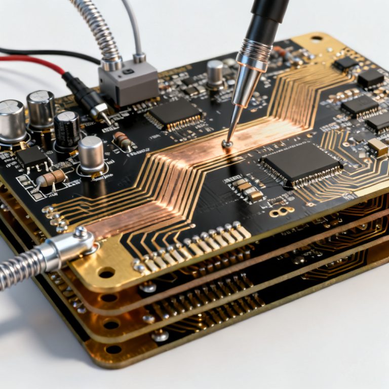
In high-speed PCB design, stitching vias for return path continuity are essential to minimize loop inductance and ensure signal integrity. When a signal transitions between layers, the return current must follow a low-impedance path; without proper stitching vias, large loop areas form, increasing EMI and degrading performance.
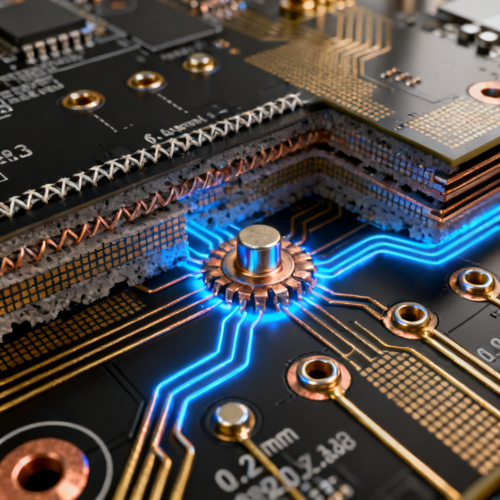
The Physics of Return Current and Why Stitching Vias Matter
The Principle of Least Inductance
At high frequencies, return current follows the path of least inductance, which lies directly under the signal trace in the reference plane. When a signal via changes layers, a stitching via placed nearby provides this low-inductance path. Without it, the return current must travel through plane edges or decoupling capacitors, creating a large loop.
The Loop Area Problem
Loop area is the most critical EMI metric. A larger loop acts as a more efficient antenna for emission and susceptibility. The formula E ∝ I × f² × A shows that reducing loop area via stitching vias is fundamental for high-speed PCB design.
What Happens Without Stitching Vias
- Increased EMI leading to compliance failures
- Signal integrity degradation from impedance mismatch
- Ground bounce from multiple signals sharing poor return paths
- Crosstalk through shared ground plane impedance
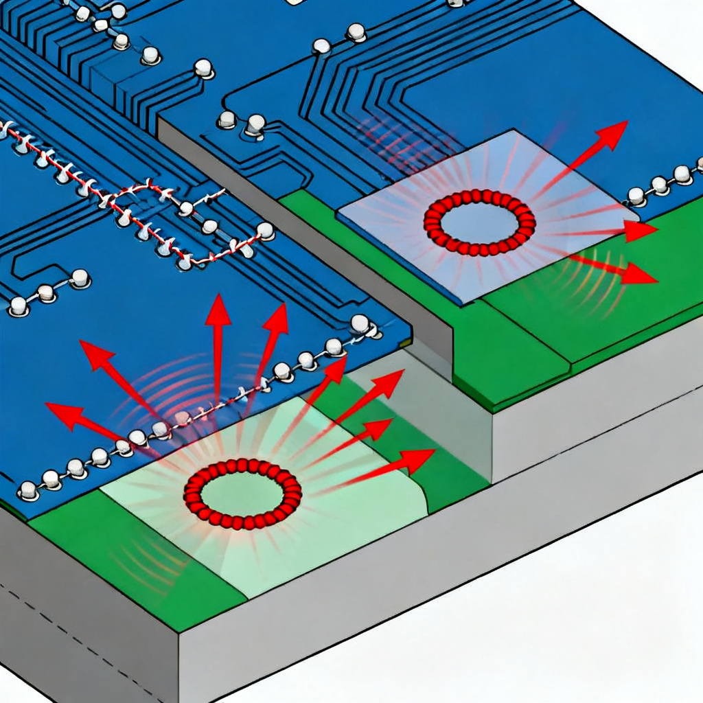
Where to Place Stitching Vias – The Golden Rules
Proximity to the Signal Via (The “1mm Rule”)
Place a stitching via within 1 mm (40 mils) of the signal via, ideally 0.5 mm. This minimizes lateral distance in the ground plane, reducing loop inductance. For differential pairs, use two stitching vias symmetrically.
Along the Entire Trace Length
For traces running adjacent to ground plane splits, place stitching vias at every λ/20 of the highest signal frequency. For a 1 GHz signal, this means every 7.5 mm.
At the Edges of Ground Plane Splits
Bridge ground plane splits with a row of stitching vias spaced at λ/20 or less. Never route a high-speed signal across a split in its reference plane.
Around the Periphery of the PCB
Create a Faraday cage by placing stitching vias every 1–3 mm around the board edge. This reduces radiated emissions from board edges.
Near Connectors and I/O
Place stitching vias immediately adjacent to each signal pin of high-speed connectors, connecting ground pins to internal planes for low-impedance return paths.
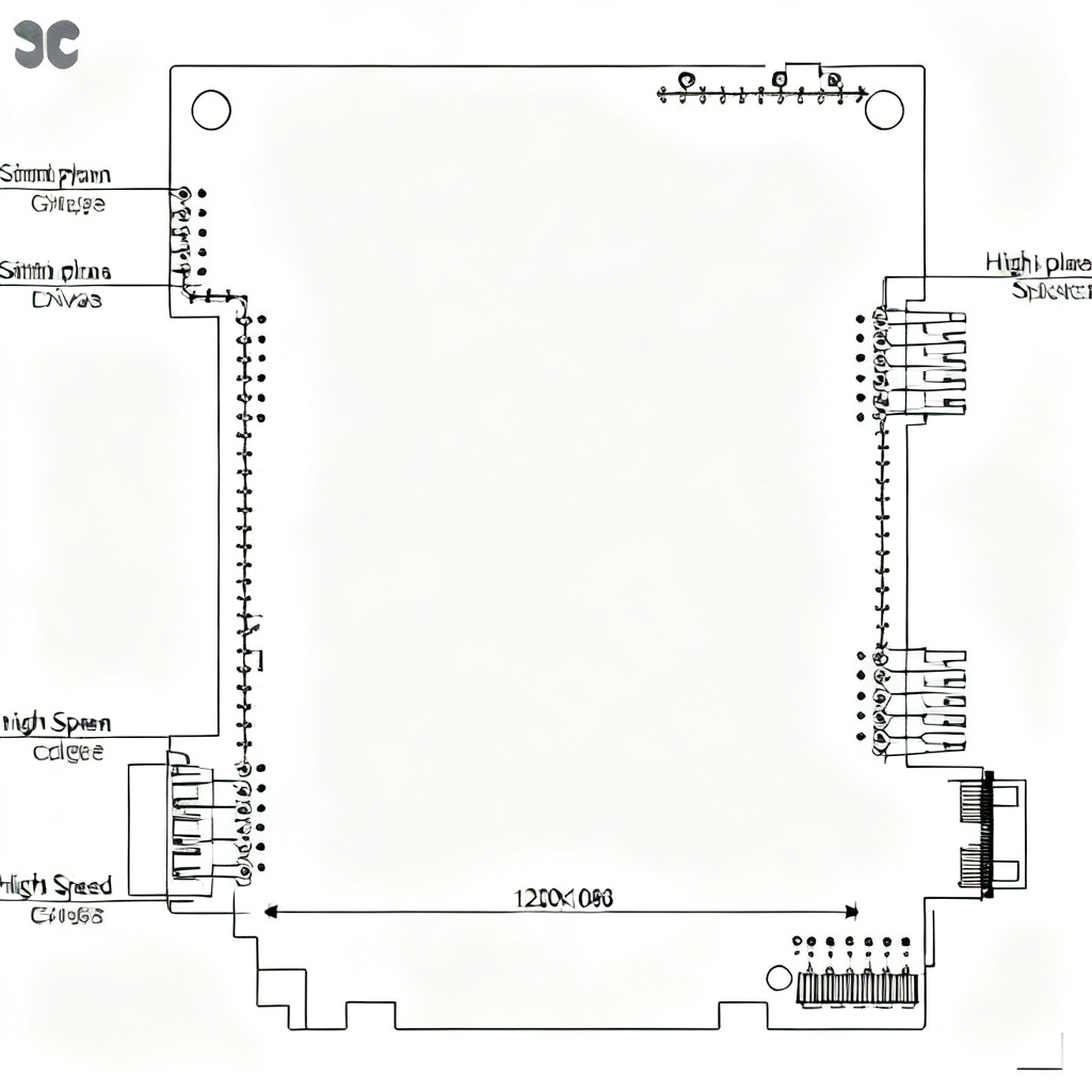
How Many Stitching Vias – The Quantitative Approach
The Inductance Model
A single via has 0.5–1.5 nH inductance. Multiple vias in parallel reduce total inductance by L_total = L_via / N. Mutual inductance slightly reduces this benefit but the rule is useful for initial design.
Determining the Required Inductance
Keep return path impedance below 1 ohm at the highest frequency. For a 5 GHz signal with single via inductance of 1 nH, you need approximately 31 vias to reach below 1 ohm. For most designs below 1 GHz, 3–5 vias per signal via transition are sufficient.
Empirical Rules from Industry Leaders
- Use a minimum of 3 stitching vias in a triangular pattern around a single signal via
- For differential pairs, use 4 stitching vias (2 per signal via)
- For high-current power delivery, use 6–8 vias in a ring
- For ground plane splits, use as many vias as physically possible at λ/20 spacing
Advanced Considerations and Best Practices
Via Geometry and Its Impact
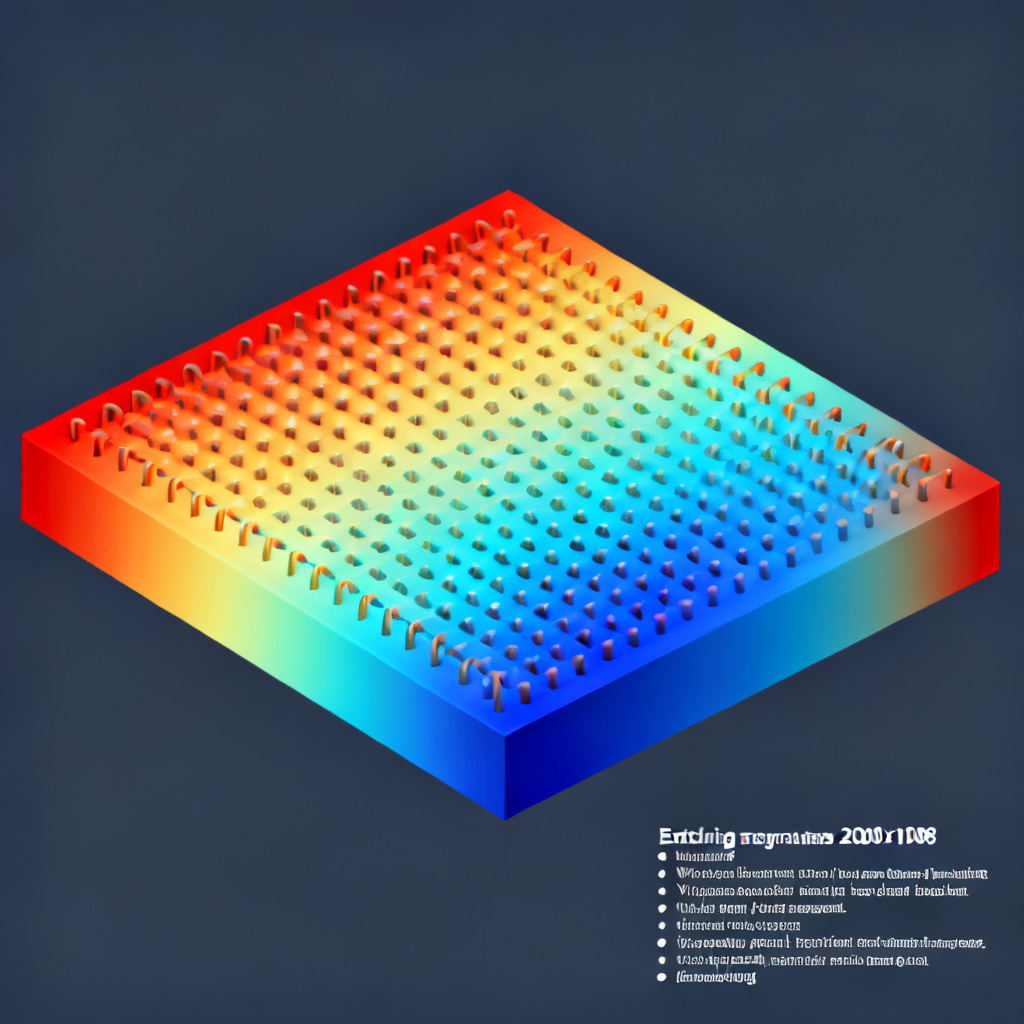
Larger diameter vias have lower inductance but consume more area. Shorter vias (using microvias) reduce inductance. Keep antipads as small as fabrication tolerances allow. Stitch all available ground layers for critical paths.
Simulation and Verification
Use 3D EM simulation tools to model return path impedance. A well-designed stitching via array should have return loss (S11) below -20 dB across the frequency band of interest.
Stitching Vias for Power Planes
When a signal references a power plane, provide stitching vias between the power plane and ground at the transition point, often using a parallel pair of vias.
Manufacturing Constraints
Minimum center-to-center spacing is typically 0.8–1.0 mm; for tighter spacing, use HDI microvias. Consider conductive epoxy fill for high-reliability designs. Avoid tenting critical stitching vias.
Case Studies and Common Mistakes
Case Study 1: The 10 Gbps SerDes Failure
A single stitching via 3 mm away caused 2 nH loop inductance and 15 dB excess emissions. Adding three vias within 0.5 mm reduced inductance to 0.3 nH and solved the issue.
Case Study 2: The RF Power Amplifier
A ground plane split without stitching vias caused 3 dB gain ripple. Adding 20 vias at λ/20 spacing reduced ripple to 0.2 dB.
Common Mistakes
- Using only one stitching via – always use at least three
- Placing vias too far from the signal via – aim for 0.5 mm or less
- Ignoring via stitching for power planes – stitch power to ground at transitions
- Over-stitching without simulation – use simulation to determine optimal count
Stitching Vias for Return Path: Practical Checklist
- Identify all signal via transitions for high-speed traces
- Place at least 3 stitching vias within 1 mm (preferably 0.5 mm) of each signal via
- For differential pairs, use 4 stitching vias (2 per signal via)
- For ground plane splits, place a row at λ/20 spacing
- For board edges and connectors, add a fence every 1–3 mm
- Calculate required number using inductance formula for frequencies above 5 GHz
- Simulate via transition to verify return loss below -20 dB
- Check manufacturing constraints for spacing and aspect ratio
Comparison: Stitching Via Strategies for High-Speed PCB
| Parameter | Single Via | 3 Vias in Triangle | 6 Vias in Ring |
|---|---|---|---|
| Inductance at 1 GHz | ~1.5 nH | ~0.5 nH | ~0.25 nH |
| Loop Area (relative) | 100% | 33% | 17% |
| EMI Reduction | Baseline | ~10 dB | ~15 dB |
| Best For | Low-speed signals | High-speed digital (1-5 GHz) | RF, microwave, high-current |
Glossary of Key Terms
- Stitching via: A via connecting ground planes to provide a low-impedance return path
- Return path: The path taken by return current in a reference plane
- Loop inductance: Inductance of the return current loop, minimized by proper stitching
- λ/20 spacing: Maximum distance between vias to maintain effective ground plane continuity
Frequently Asked Questions
How many stitching vias do I need for a high-speed PCB design?
For most high-speed PCB designs below 5 GHz, use at least 3 stitching vias per signal via transition. For frequencies above 10 GHz, calculate using the inductance formula to determine the exact number.
What is the optimal distance for placing a stitching via?
The optimal distance is less than 1 mm (40 mils) from the signal via, with 0.5 mm (20 mils) being ideal for frequencies above 5 GHz.
Can I use stitching vias for power planes?
Yes, when a signal references a power plane, stitch the power plane to ground at the transition point using a parallel pair of vias.
Do stitching vias affect manufacturing cost?
Adding many vias can increase cost, but simulation helps determine the minimum needed. Most standard PCB manufacturers handle 0.8 mm spacing without premium charges.
What happens if I place stitching vias too far apart?
Excessive spacing increases loop inductance, leading to higher EMI, signal integrity degradation, and potential compliance failures.