Crosstalk and EMI in eye diagram PCB analysis are critical for diagnosing signal integrity issues in high-speed designs. This guide explains how external interference distorts the eye pattern and provides expert techniques for identification and mitigation.
Eye Diagram Basics for Crosstalk and EMI in Eye Diagram PCB
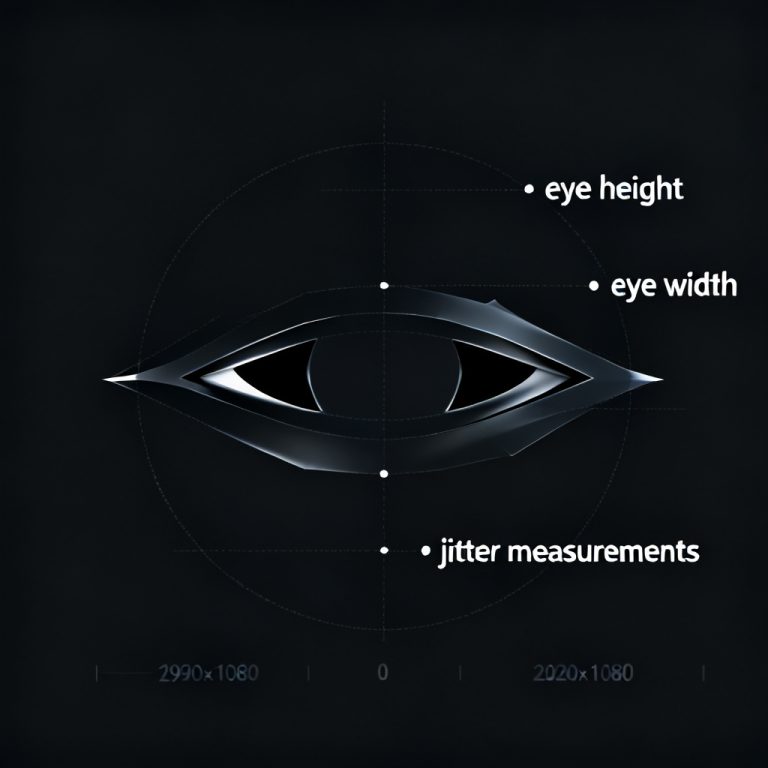
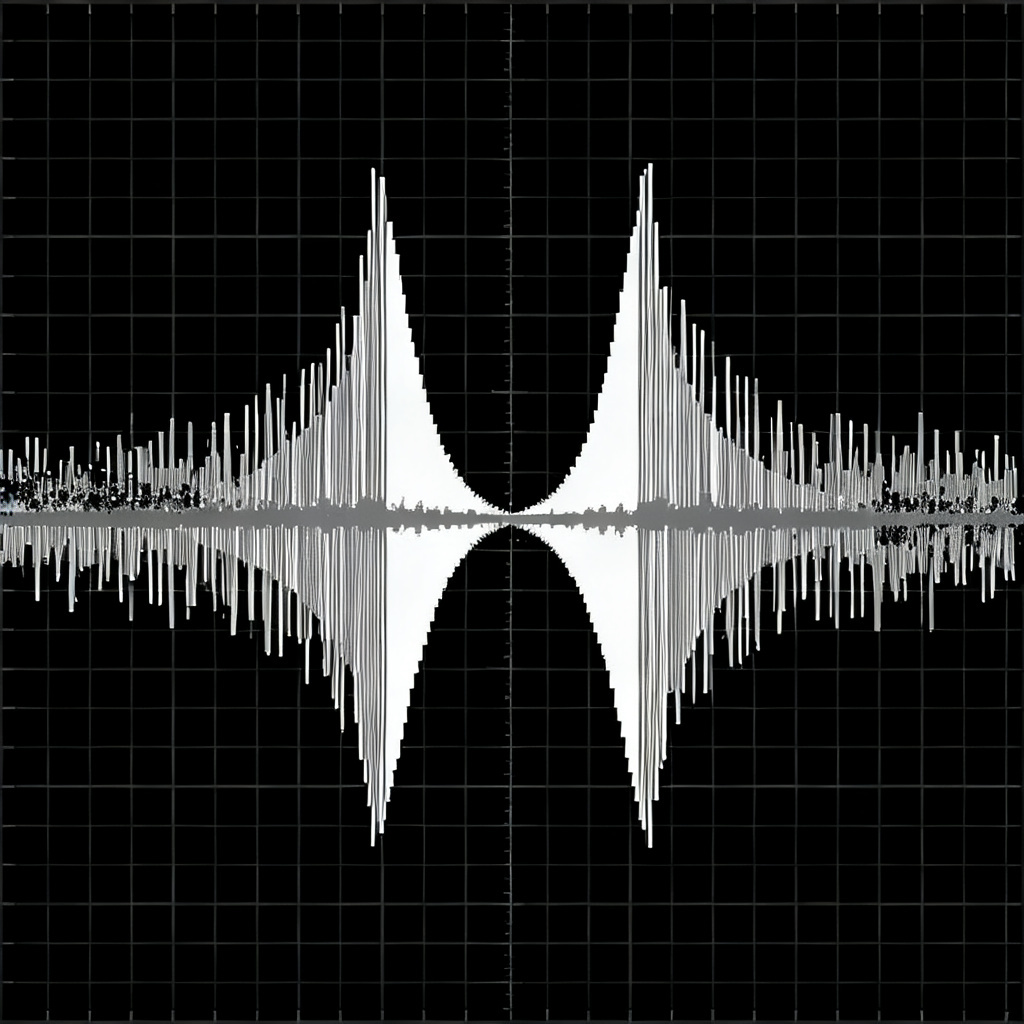
An eye diagram is created by overlaying multiple digital transitions on an oscilloscope. The resulting eye reveals the health of a high-speed channel. Key metrics include eye height, eye width, jitter, and rise/fall times. Both crosstalk and EMI degrade these parameters, closing the eye and increasing bit error rates.
Key Metrics Affected by Crosstalk and EMI
- Eye Height: Reduced by crosstalk voltage injection or EMI noise floor.
- Eye Width: Narrowed by jitter from both crosstalk and EMI.
- Jitter: Pattern-dependent for crosstalk; random for EMI.
- Rise/Fall Time: Slower edges reduce EMI susceptibility but may increase timing uncertainty.
Crosstalk in Eye Diagram PCB: Causes and Identification
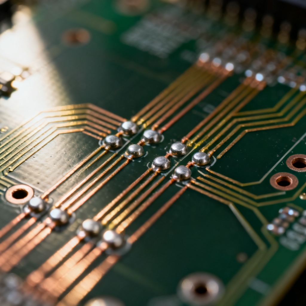
Crosstalk occurs when an electromagnetic field from an aggressor trace couples onto a victim trace. This deterministic interference appears in the eye diagram as asymmetric distortion, pattern-dependent jitter, or a double-eye effect.
Types of Crosstalk in High-Speed PCBs
| Crosstalk Type | Coupling Mechanism | Eye Diagram Signature |
|---|---|---|
| Capacitive Crosstalk | Electric field between parallel traces | Asymmetric eye closure, reduced height |
| Inductive Crosstalk | Magnetic field from disrupted return path | Broad noise pulse, jitter increase |
| Forward Crosstalk (FEXT) | Propagates in same direction as aggressor | One-sided eye narrowing |
| Backward Crosstalk (NEXT) | Propagates toward driver | Vertical eye closure, pattern-dependent jitter |
Identifying Crosstalk in the Eye Diagram
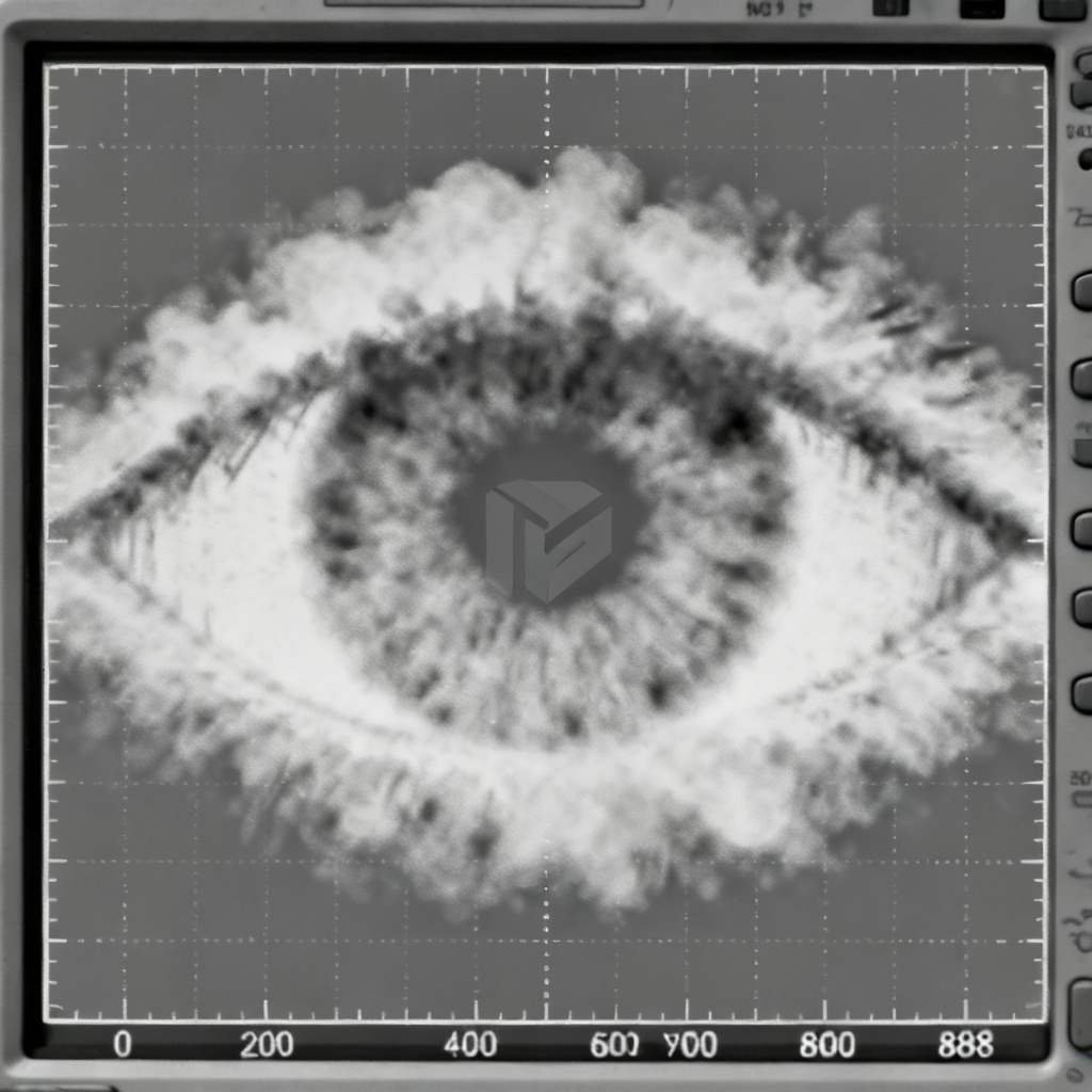
Look for asymmetric eye closure where one side of the eye is narrower than the other. Use a Bit Error Rate Tester (BERT) with PRBS patterns; if errors increase with specific data patterns, crosstalk is the cause. A “double eye” effect indicates severe coupling between aggressor and victim nets.
Crosstalk Mitigation Strategies
- Apply the 3W or 5W rule for trace spacing.
- Use solid ground planes for return path integrity.
- Add guard traces stitched with vias.
- Route critical nets in stripline layers.
- Reduce edge rates with slew-rate controlled drivers.
EMI in Eye Diagram PCB: Sources and Detection
Electromagnetic interference (EMI) is broadband, random noise from external sources like power supplies, radios, or adjacent equipment. In the eye diagram, EMI appears as a fuzzy, cloudy eye with reduced height and random jitter at the crossing points.
Common EMI Sources for High-Speed PCBs
- Radiated emissions from long traces or stubs.
- Conducted noise from power distribution networks.
- External radiators like Wi-Fi or Bluetooth.
Identifying EMI in the Eye Diagram
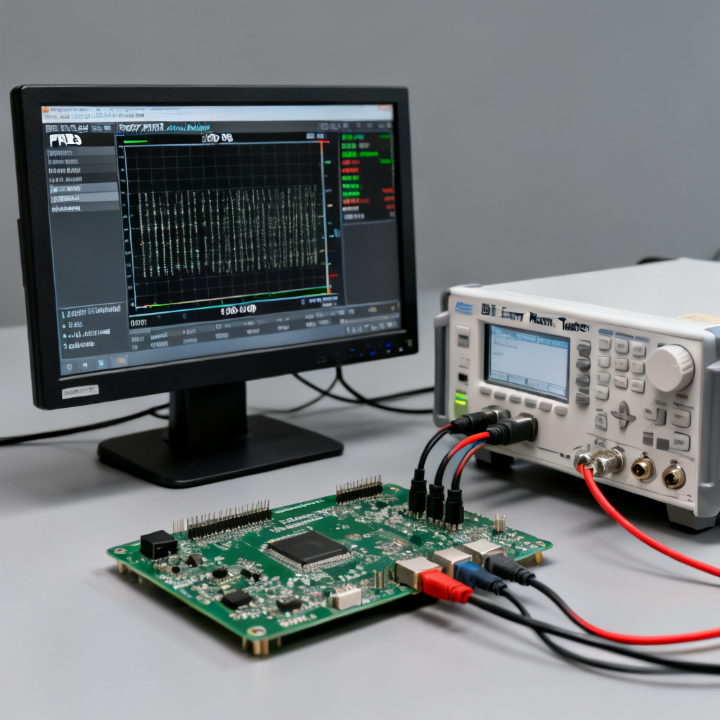
Use a spectrum analyzer to detect spikes at specific frequencies. If the eye diagram improves in a shielded chamber, external EMI is confirmed. Probe the power distribution network for ripple at switching regulator frequencies.
EMI Mitigation Strategies
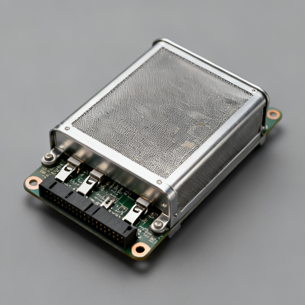
- Use metal shielding cans over sensitive sections.
- Add ferrite beads and common-mode chokes on I/O lines.
- Ensure continuous return paths under every signal.
- Apply spread spectrum clocking to reduce peak emissions.
- Use 45-degree or curved traces instead of 90-degree corners.
Crosstalk vs EMI: Distinguishing in the Eye Diagram
| Feature | Crosstalk in Eye Diagram PCB | EMI in Eye Diagram PCB |
|---|---|---|
| Nature of Jitter | Deterministic, pattern-dependent | Random, Gaussian |
| Eye Closure Pattern | Asymmetric, one side narrower | Symmetric, uniform fuzziness |
| Frequency Dependency | Tied to data rate and pattern | Any frequency (e.g., 60 Hz, 2.4 GHz) |
| Test Method | BERT with PRBS patterns | Spectrum analyzer or shielded chamber |
| Root Cause | Adjacent traces, broken return path | External radiators, poor shielding |
If the eye diagram degrades only when a specific neighboring trace is active, it is crosstalk. If degradation is constant regardless of board activity, suspect EMI.
Advanced Identification Techniques for Crosstalk and EMI in Eye Diagram PCB
Bit Error Rate Tester (BERT)
A BERT sends a known PRBS pattern and counts errors. Crosstalk causes errors at specific bit transitions; EMI causes random errors. This distinction is key for targeted mitigation.
Time Domain Reflectometry (TDR)
TDR identifies impedance discontinuities from crosstalk coupling points. A dip in the impedance profile at a specific trace location suggests a coupling issue.
Eye Mask Testing
Industry standards define an eye mask—a forbidden region. Crosstalk often violates the mask vertically; EMI violates it horizontally due to jitter.
Practical Checklist for High-Speed PCB Design
| Requirement | Description |
|---|---|
| Controlled Impedance Stackup | Specify a 4+ layer stackup with ground planes for signal integrity. |
| Simulation Reports | Request pre-layout simulation showing eye diagram performance. |
| Ground Plane Stitching | Ensure contiguous ground reference under all high-speed traces. |
| Differential Pair Routing | Require 100Ω impedance with 5x trace width spacing. |
| EMI Filtering on I/O | Specify common-mode chokes and ferrite beads on external connectors. |
| Post-Manufacturing Testing | Insist on eye diagram testing at maximum operating frequency. |
FAQ: Crosstalk and EMI in Eye Diagram PCB
What is the main difference between crosstalk and EMI in the eye diagram?
Crosstalk is deterministic and pattern-dependent, causing asymmetric eye closure and pattern-dependent jitter. EMI is random and broadband, causing symmetric fuzziness and random jitter in the eye diagram of a high-speed PCB.
How can I identify crosstalk in my eye diagram?
Look for asymmetric eye closure, pattern-dependent jitter, or a ‘double eye’ effect. Use a BERT with PRBS patterns to isolate crosstalk from EMI in your high-speed PCB design.
What mitigation strategies reduce crosstalk in high-speed PCBs?
Increase trace spacing (3W or 5W rule), use ground plane shielding, add guard traces, optimize layer stackup with stripline routing, and slow down edge rates to reduce crosstalk in the eye diagram.
How does EMI appear in the eye diagram?
EMI appears as a fuzzy, cloudy eye with reduced height and widened, fuzzy crossing points. It adds random jitter and can be identified using a spectrum analyzer or shielded chamber test.
What is the role of the eye diagram in high-speed PCB design?
The eye diagram is the industry-standard metric for assessing signal quality. It reveals eye height, eye width, jitter, and rise/fall times, helping diagnose crosstalk and EMI in high-speed PCBs.
Glossary: Key Terms for Crosstalk and EMI in Eye Diagram PCB
- BERT: Bit Error Rate Tester, used to measure digital signal quality.
- Deterministic Jitter: Bounded jitter from crosstalk or other predictable sources.
- FEXT: Far-End Crosstalk, coupling that propagates to the receiver end.
- NEXT: Near-End Crosstalk, coupling that propagates back to the driver.
- PRBS: Pseudo-Random Binary Sequence, a test pattern for signal integrity.
- TDR: Time Domain Reflectometry, used to measure impedance discontinuities.