Duty Cycle Distortion in High Speed PCB is a critical signal integrity issue caused by rise and fall time mismatch, degrading system performance in serial data links and clock distribution networks. This comprehensive guide explores root causes, measurement techniques, and mitigation strategies for high-speed designs.
Understanding Duty Cycle Distortion in High Speed PCB
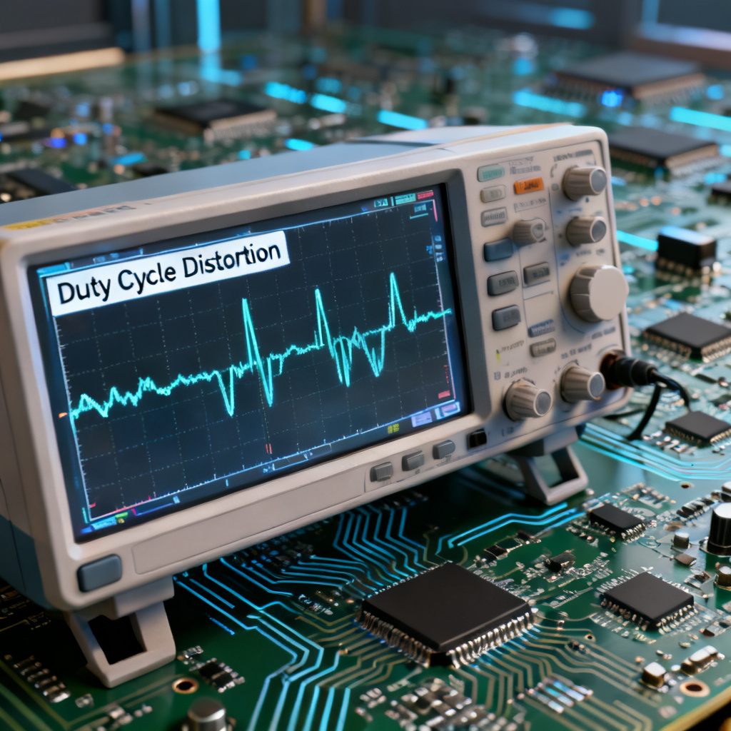
Duty cycle distortion in High Speed PCB refers to the deviation of a signal’s duty cycle from its ideal 50% mark, manifesting as pulse width variation. This deterministic jitter reduces timing margin and increases bit error rates (BER) in protocols like PCIe, USB, and Ethernet. The root cause is asymmetry between rise time (Tr) and fall time (Tf), originating from driver mismatch, parasitic elements, and impedance discontinuities. Other contributing factors include threshold offsets in receivers and asymmetrical PCB trace geometry, but Tr/Tf imbalance remains primary.
The Physics of Rise and Fall Time Mismatch in PCB
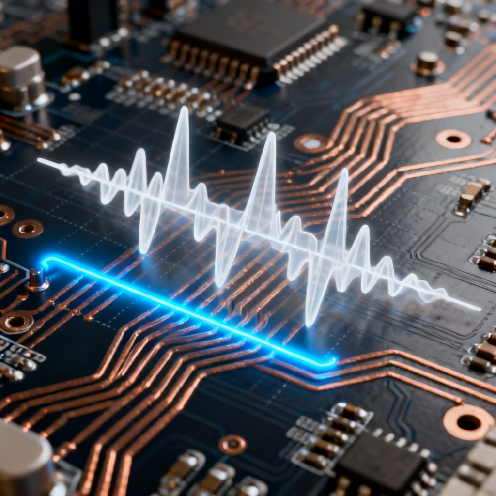
To grasp duty cycle distortion in High Speed PCB, we must examine physical mechanisms causing Tr/Tf differences. High-speed signals interact with driver characteristics, PCB materials, and layout parasitics.
Driver Output Impedance and Slew Rate
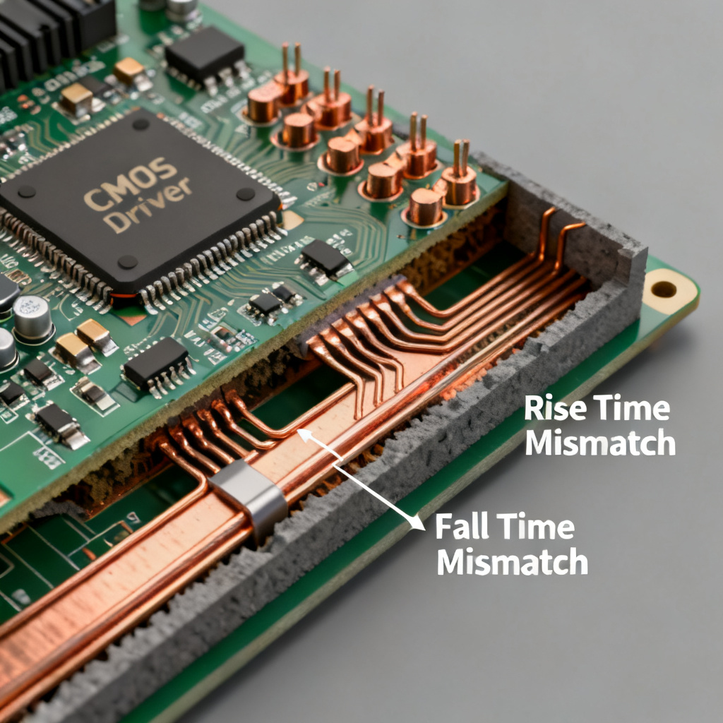
The output stage of a CMOS driver has mismatched PMOS and NMOS on-resistance (Ron), e.g., 10 ohms for rising edge vs. 15 ohms for falling edge. This imbalance, frequency-dependent and worsening at higher speeds, directly contributes to duty cycle distortion in High Speed PCB.
Parasitic Capacitance and Inductance
PCB traces, via stubs, and connectors introduce parasitic elements that disproportionately affect one edge. For instance, a longer via stub slows the rising edge more due to inductance’s effect on current slew rate, exacerbating duty cycle distortion in High Speed PCB.
Transmission Line Effects
Impedance discontinuities cause reflections that alter receiver trigger levels, artificially shifting duty cycle. A 50-ohm driver into a 60-ohm trace creates asymmetric overshoot/undershoot, worsening duty cycle distortion in High Speed PCB.
Temperature and Voltage Variations
Environmental factors like temperature and supply voltage droop affect PMOS and NMOS differently, leading to dynamic duty cycle distortion in High Speed PCB.
Measurement and Quantification of Duty Cycle Distortion
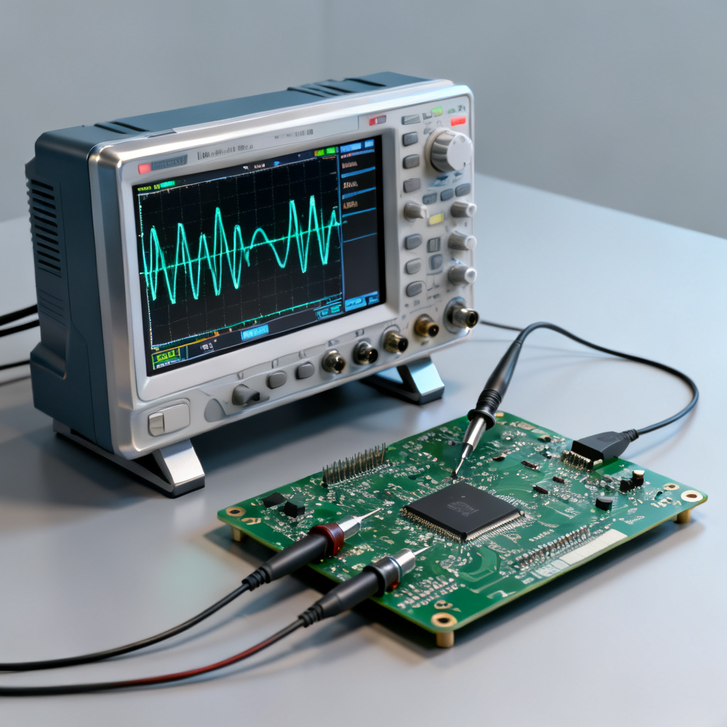
Accurate measurement is essential for diagnosing duty cycle distortion in High Speed PCB. Industry-standard techniques include real-time oscilloscope eye diagram analysis, jitter decomposition, TDR measurements, and IBIS simulation.
Using a Real-Time Oscilloscope
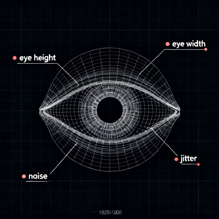
Capture a long data stream (e.g., PRBS pattern) and analyze the eye diagram. DCD appears as a horizontal shift in the crossing point. Quantify duty cycle error by measuring average high pulse width minus low pulse width, divided by total period. For a 50% duty cycle, any deviation is DCD. Tektronix and Keysight recommend at least 1 million UI for statistical accuracy.
Jitter Decomposition
Separate deterministic jitter (DJ) from random jitter (RJ). DCD is a subset of DJ. Use a jitter analysis tool to extract the DCD component. The formula is: DCD (in ps) = (Tr – Tf) / 2, assuming linear transition and equal thresholds. More precisely, DCD = (t_high_avg – t_low_avg) / 2.
TDR Measurements
For PCB characterization, TDR reveals impedance mismatches causing DCD. Measure 10%-90% rise and fall times at the receiver end. A difference of more than 10% between Tr and Tf (e.g., Tr=50 ps, Tf=45 ps) indicates a potential DCD issue.
Simulation with IBIS Models
Before fabrication, use IBIS models to simulate Tr and Tf. Compare the driver’s output waveform at the package pin and receiver. Any asymmetry in slew rate or overshoot/undershoot will manifest as DCD.
Impact on System Performance
Duty cycle distortion in High Speed PCB degrades system reliability in measurable ways:
- Eye Diagram Closure: A 5-ps DCD in a 10 Gbps system (100 ps UI) reduces eye opening by 10%, increasing BER from 10^-12 to 10^-6.
- Clock Jitter and Skew: A 2-ps DCD can cause 1-ps jitter in the clock tree, unacceptable for 28 Gbps links.
- Data Pattern Dependence: Long runs of identical bits cause baseline wander, interacting with Tr/Tf mismatch to exacerbate DCD.
- EMI and Power Integrity: Asymmetric edges generate odd-order harmonics increasing EMI, and uneven current draw causes voltage ripple.
Mitigation Strategies for Rise/Fall Time Mismatch
To combat duty cycle distortion in High Speed PCB, designers must address both driver and PCB layout levels.
At the Driver Level
- Select Drivers with Balanced Slew Rates: Choose ICs with matched PMOS/NMOS drive strengths. Look for datasheets specifying “slew rate matching” or “duty cycle correction.”
- Use Pre-Emphasis or Equalization: Pre-emphasis boosts high-frequency components compensating for slower rise times. De-emphasis reduces overshoot on the falling edge.
- Adjust Output Impedance: Use programmable output impedance to match trace Z0, balancing Tr and Tf.
At the PCB Level
- Maintain Consistent Impedance: Design traces with controlled impedance (e.g., 50 ohms ±5%) using appropriate stackup. Avoid 90-degree corners.
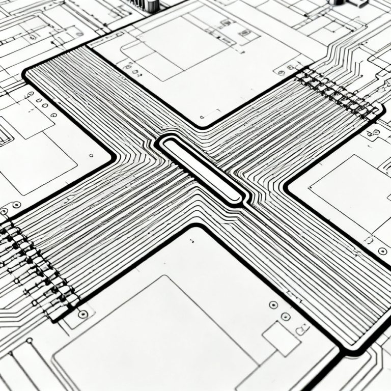
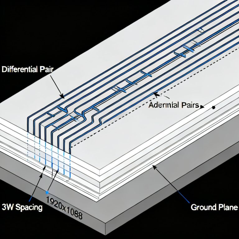
- Minimize Parasitic Elements: Keep traces short and direct. Reduce via count and use back-drilling to eliminate via stubs. For differential pairs, ensure length matching within 5 mils.
- Optimize Return Path: Provide a continuous ground plane under all high-speed traces. Use ground vias near signal vias.
- Termination Resistors: Place series termination close to the driver and parallel termination at the receiver to balance edges.
At the System Level
- Duty Cycle Correction Circuits: Some receivers include DLLs that adjust the sampling clock to compensate for up to 10% DCD.
- AC Coupling with Care: Ensure the time constant is >10x the longest run of identical bits to prevent baseline wander.
- Thermal Management: Use heat sinks or airflow to keep driver temperature stable, as temperature gradients worsen Tr/Tf mismatch.
Advanced Topics and Real-World Examples
Case Study: 25 Gbps NRZ Link with DCD
A design using a 25 Gbps NRZ transceiver exhibited a BER of 10^-8. Eye diagram analysis revealed a 3-ps DCD. Investigation showed the driver had a Tr of 12 ps and Tf of 15 ps, a 25% mismatch. After switching to a driver with matched slew rates (Tr=13 ps, Tf=13.5 ps), DCD dropped to 1 ps, and BER improved to 10^-12.
DCD in Differential Signaling (e.g., LVDS)
In differential pairs, DCD can arise from skew between P and N signals. Mitigation includes tight length matching (within 1 ps) and using symmetrical layout.
Simulation Tools and Software
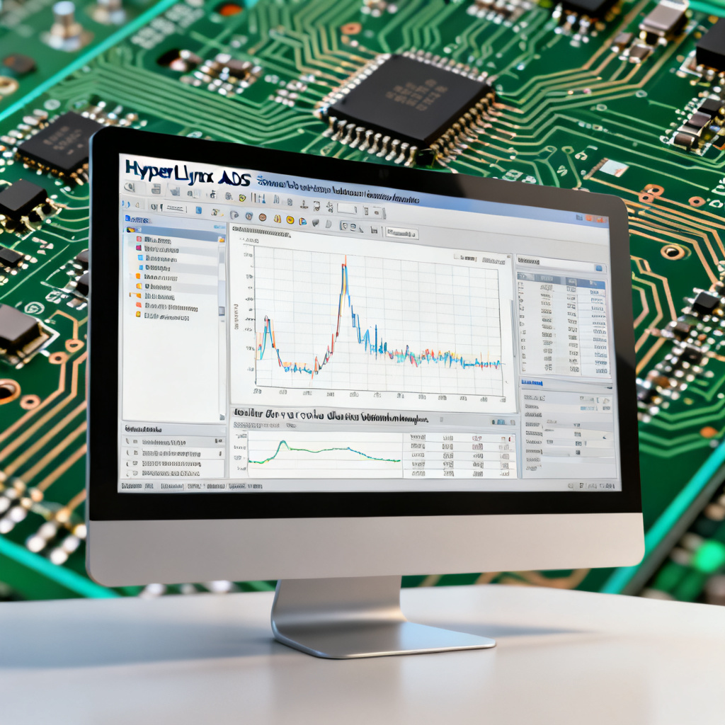
| Tool | Application for Duty Cycle Distortion in High Speed PCB |
|---|---|
| HyperLynx | Pre-layout simulation of Tr/Tf mismatch |
| ADS (Advanced Design System) | Jitter decomposition and eye analysis |
| Altium Designer | Impedance-controlled routing and stackup planning |
Frequently Asked Questions About Duty Cycle Distortion in High Speed PCB
What is duty cycle distortion in High Speed PCB?
Duty cycle distortion in High Speed PCB is a timing error where the signal’s high and low pulse widths deviate from the ideal 50% ratio, caused primarily by rise and fall time mismatch.
How does rise and fall time mismatch cause duty cycle distortion in High Speed PCB?
When rise time (Tr) and fall time (Tf) are unequal, the signal crosses the threshold at different points, shifting the duty cycle. This is the primary mechanism of duty cycle distortion in High Speed PCB.
What are common mitigation techniques for duty cycle distortion in High Speed PCB?
Common techniques include selecting drivers with balanced slew rates, maintaining consistent impedance, minimizing via stubs, using pre-emphasis, and implementing duty cycle correction circuits.
How is duty cycle distortion in High Speed PCB measured?
It is measured using real-time oscilloscopes for eye diagram analysis, jitter decomposition software, TDR for impedance characterization, and IBIS simulation for pre-layout validation.
What is the impact of duty cycle distortion in High Speed PCB on system performance?
It reduces timing margin, closes the eye diagram, increases BER, introduces clock jitter, and can cause EMI issues. In high-speed links like PCIe or Ethernet, even small DCD leads to significant degradation.
Call to Action: Partner with Experts for Your High-Speed PCB Needs
At [Your Company Name], we specialize in high-speed PCB design and manufacturing, focusing on minimizing signal integrity issues like duty cycle distortion in High Speed PCB. Our team uses advanced simulation tools (e.g., HyperLynx, ADS) and rigorous fabrication processes (e.g., tight impedance tolerance, back-drilling) to ensure your designs achieve first-pass success. Whether you need a prototype for a 25 Gbps link or a production run for a complex multi-layer board, we deliver High-Speed PCBs with Optimized Rise/Fall Times.
Get Your Free Design Review Today
Contact us at [email/phone] or visit [website] to submit your design files. We’ll analyze your PCB for DCD risks and provide actionable recommendations—no obligation. Let’s build reliable, high-performance electronics together.
Glossary of Key Terms
- DCD: Duty Cycle Distortion
- Tr/Tf: Rise Time / Fall Time
- UI: Unit Interval (bit period)
- BER: Bit Error Rate
- IBIS: I/O Buffer Information Specification
- DLL: Delay-Locked Loop