In high-speed PCB design, Deterministic Jitter (DJ) is the bounded, predictable timing error that directly limits signal integrity at multi-gigabit data rates. Unlike random jitter, DJ originates from identifiable sources like impedance mismatches, driver asymmetry, and power supply noise, making it a critical focus for reliable data transmission. Understanding its three dominant subtypes—Intersymbol Interference (ISI), Duty Cycle Distortion (DCD), and Periodic Jitter (Pj)—enables engineers to systematically diagnose and eliminate timing errors in their PCB layouts.
Introduction: The Critical Role of Deterministic Jitter in High-Speed Design
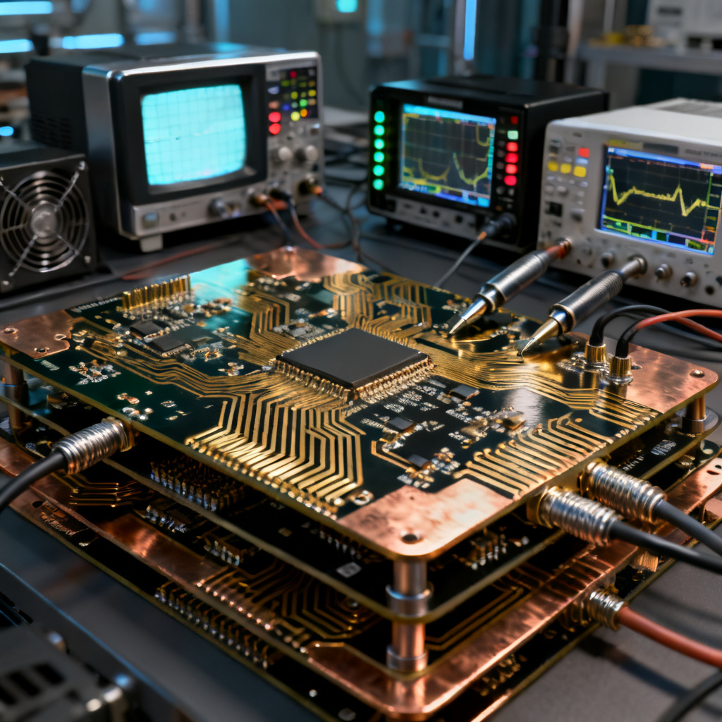
In high-speed PCB design, as data rates soar into the multi-gigabit per second range, the margin for timing errors shrinks dramatically. Total jitter (TJ) is the ultimate enemy of reliable data transmission, and it is composed of two primary components: Random Jitter (RJ) and Deterministic Jitter (DJ). While RJ is unbounded and Gaussian, Deterministic Jitter is bounded, predictable, and originates from specific, identifiable sources within the system.
Understanding DJ is not just an academic exercise; it is the cornerstone of effective PCB design and debugging. Unlike RJ, which can only be managed through statistical budgeting, DJ can be measured, traced, and eliminated. This pillar content provides a complete breakdown of DJ, focusing on its three dominant subtypes: Intersymbol Interference (ISI), Duty Cycle Distortion (DCD), and Periodic Jitter (Pj). We explore their root causes, identification in measurements, and mitigation strategies for your high-speed PCB layout and stackup.
What is Deterministic Jitter? A Deep Dive
The Core Definition
Deterministic Jitter is the component of total timing jitter that is bounded, predictable, and non-Gaussian. Its peak-to-peak amplitude has a definitive limit, unlike the theoretical infinite tail of Random Jitter. This bounded nature means that if you can identify and eliminate the root cause, the jitter disappears. DJ is typically caused by electromagnetic interference (EMI), crosstalk, power supply noise, signal reflections, and switching characteristics of the driver and receiver.
The DJ Family Tree
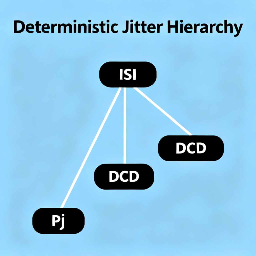
DJ is further categorized into two main branches:
- Correlated Jitter: Jitter that is related to the data pattern being transmitted. This includes ISI (which is data-dependent) and DCD (which is duty-cycle dependent).
- Uncorrelated Jitter: Jitter that is not related to the data pattern. The primary subtype here is Periodic Jitter (Pj), often caused by external clock sources or power supply ripple.
Why DJ is More Dangerous Than RJ in Design
While RJ sets the fundamental noise floor, DJ often determines the deterministic error floor of a link. Because DJ is bounded, its peak-to-peak value can be directly subtracted from the total timing budget. A high DJ value directly reduces the eye-opening, making the system more susceptible to bit errors. In practice, a design with excessive DJ will fail even if the RJ budget is perfectly met. Therefore, mastering DJ is the most direct path to a robust, high-yield product.
Intersymbol Interference (ISI) – The Data Pattern Villain
ISI is the most common and often the most challenging form of DJ to mitigate. It occurs when the characteristics of the transmission channel (the PCB trace, via, connector) cause the energy of one bit to bleed into subsequent bits, interfering with their detection.
The Physics of ISI
The root cause of ISI is channel bandwidth limitation and impedance discontinuities.
- Bandwidth Limitation: A real PCB trace acts as a low-pass filter. High-frequency components of a fast signal (the sharp edges of a 0101 pattern) are attenuated more than low-frequency components (the long, flat levels of a 0000 or 1111 pattern). When a long string of identical bits (e.g., five 1s) is transmitted, the channel charges up to a higher voltage level. When a single 0 follows, the channel cannot discharge quickly enough, and the 0 appears at a higher voltage than it should – a classic ISI effect.
- Impedance Discontinuities: Reflections caused by vias, connectors, or impedance mismatches create secondary pulses that arrive at the receiver at different times. These reflections interfere with the main signal, causing the voltage level of the current bit to be distorted based on the state of previous bits.
Identifying ISI in Measurements
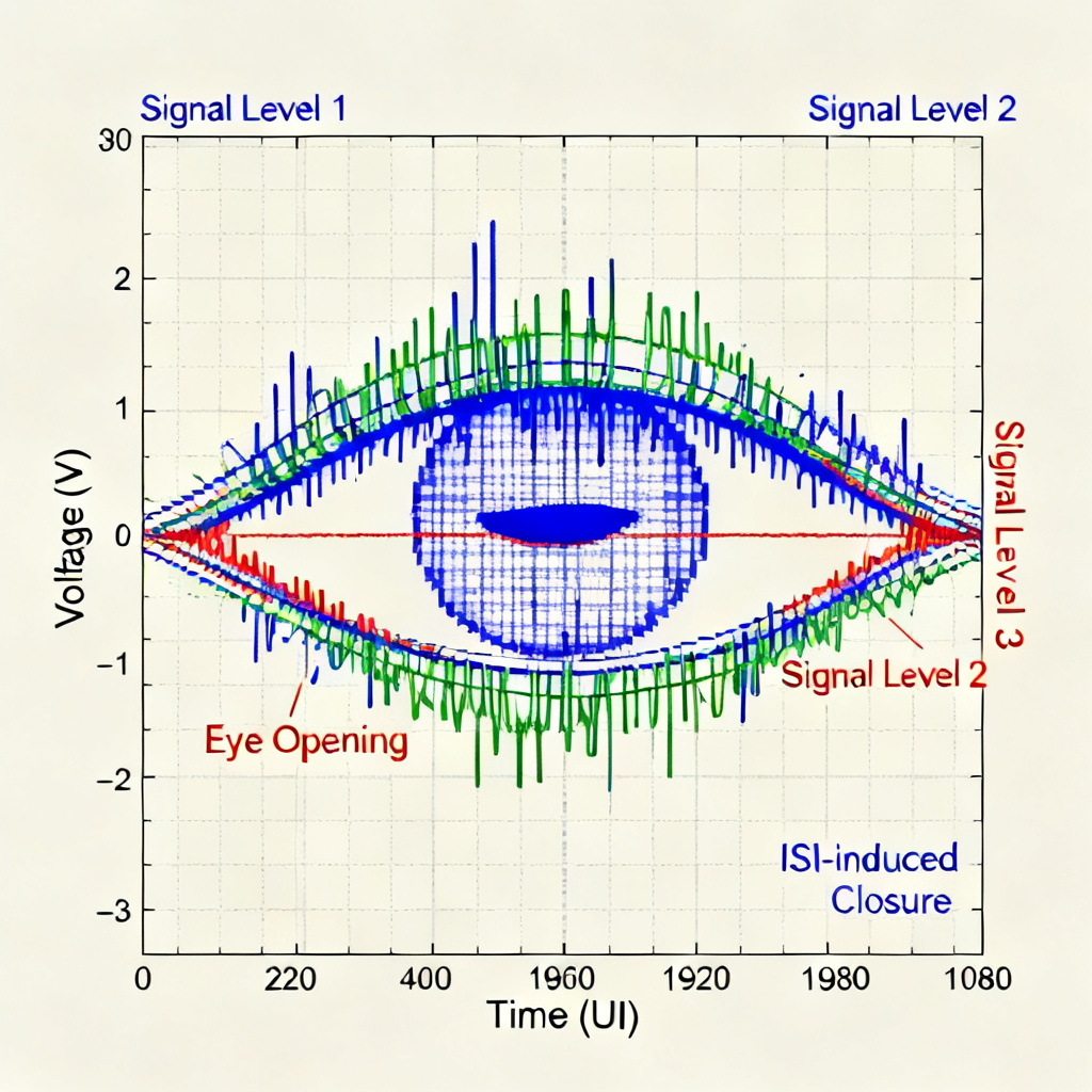
ISI is best observed in a Tektronix or Keysight sampling oscilloscope using a Persistence Map or Eye Diagram.
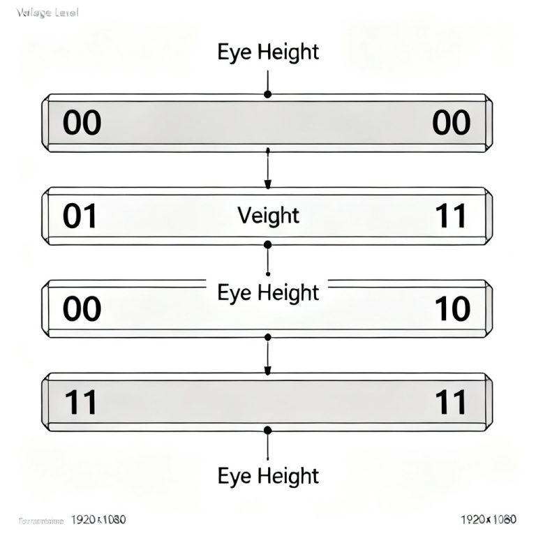
- Eye Diagram Signature: An eye diagram dominated by ISI shows multiple, distinct voltage levels at the crossing point (the center of the eye). Instead of a clean, single crossing line, you will see a fuzzy or double-humped distribution. The eye opening will be vertically closed, and the jitter histogram will show a bimodal or multimodal distribution, corresponding to different data patterns (e.g., a 0001 pattern vs. a 1110 pattern).
- Bathtub Curve: In a BER bathtub curve, ISI manifests as a rapid, steep slope on both sides of the curve, creating a narrow flat region in the center. This indicates that the deterministic component is dominating the jitter budget.
Mitigation Strategies for ISI
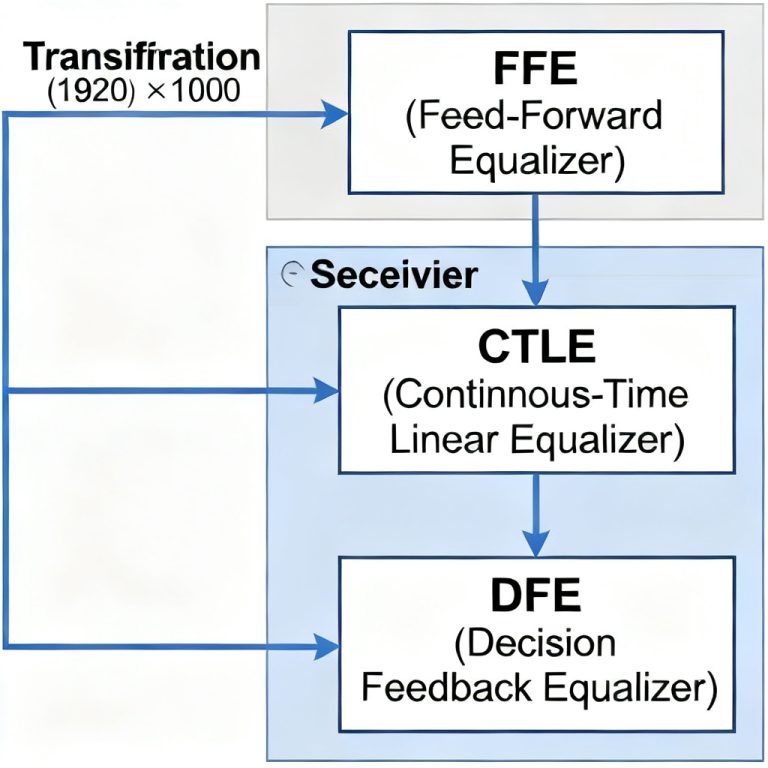
- Channel Equalization: This is the most powerful tool. Feed-Forward Equalization (FFE) at the transmitter pre-emphasizes high-frequency components (boosting the first bit after a transition). Continuous Time Linear Equalization (CTLE) and Decision Feedback Equalization (DFE) at the receiver actively cancel post-cursor ISI.
- Improve Channel Bandwidth: Reduce trace length, use lower-loss dielectrics (e.g., Rogers 4350B, Megtron 6), and minimize the number of vias. Use wider traces to reduce conductor loss.
- Impedance Matching: Ensure a clean, continuous 50-ohm (or 100-ohm differential) impedance path from driver to receiver. Use proper termination and minimize stub lengths on vias.
- Pre-Emphasis and De-Emphasis: Many high-speed transceivers offer adjustable pre-emphasis (boost the first bit) or de-emphasis (reduce the amplitude of subsequent bits) to pre-compensate for the channel’s low-pass behavior.
Duty Cycle Distortion (DCD) – The Asymmetry Issue
DCD is a form of DJ where the duration of the positive pulse (the 1 bit) is not equal to the duration of the negative pulse (the 0 bit). This asymmetry creates jitter at the clock edges.
Root Causes of DCD
- Driver Asymmetry: The most common cause. The rise time (tR) and fall time (tF) of the output driver are not perfectly matched. If the driver turns on faster than it turns off, the pulse will be wider in one direction.
- Threshold Mismatch: The switching threshold of the receiver is not perfectly at the midpoint of the signal swing. If the threshold is too high, a 1 is detected for a shorter period than a 0. This is often caused by process variations in the silicon.
- DC Offset: Any DC offset in the signal path (e.g., from a poorly designed AC coupling capacitor or a bias voltage error) can shift the waveform relative to the receiver’s threshold, creating a DCD effect.
Identifying DCD in Measurements
- Eye Diagram Signature: DCD produces a distinctive double-line or split at the crossing point of the eye diagram. The histogram of the crossing time will show two distinct peaks, symmetric around the center. The eye will appear open but with a pronounced X-shaped crossing.
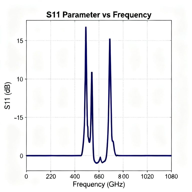
- Jitter Spectrum: In a phase noise or jitter spectrum analyzer, DCD appears as a strong, fixed component at half the data rate (e.g., at 5 GHz for a 10 Gbps signal). This is because the asymmetry repeats every two bits (a 01 or 10 pattern).
Mitigation Strategies for DCD
- Driver Calibration: Use drivers with programmable rise/fall time matching. Many modern SerDes have built-in calibration routines to equalize tR and tF.
- Receiver Threshold Adjustment: If the receiver’s threshold is adjustable, set it precisely to the midpoint of the signal swing. This is often done via on-chip calibration.
- AC Coupling: In many high-speed standards (e.g., PCIe, SATA), AC coupling capacitors are used to block DC offset. Ensure the capacitor value is large enough to not create a high-pass filter that distorts the signal but small enough to avoid long settling times.
- Duty Cycle Correction (DCC): Some clock and data recovery (CDR) circuits include a DCC loop that actively adjusts the threshold or driver to eliminate DCD.
Periodic Jitter (Pj) – The Sinusoidal Interloper
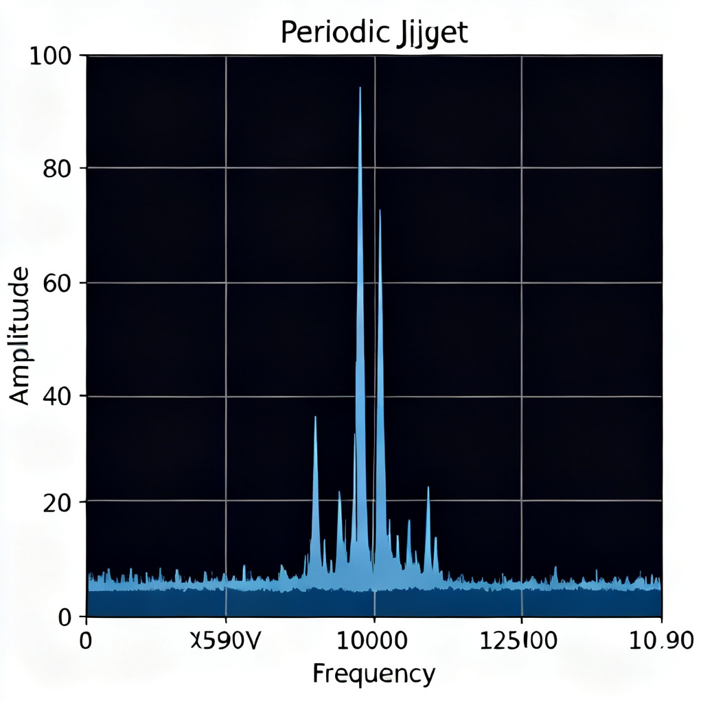
Periodic Jitter (Pj), also known as sinusoidal jitter, is an uncorrelated but bounded jitter component that repeats at a specific frequency. It is the easiest form of DJ to identify because it creates a distinct spectral line.
Sources of Periodic Jitter
- Power Supply Noise (PSN): This is the most common culprit. Ripple on the power supply rails (e.g., 100/120 Hz from a switching regulator, or high-frequency switching noise at 1-10 MHz) modulates the delay of the driver and receiver circuits, creating a sinusoidal shift in the clock edges.
- Crosstalk from Adjacent Aggressors: A strong, periodic signal on a neighboring trace (e.g., a clock line) can capacitively or inductively couple into the victim signal line, imposing a periodic jitter component.
- External EMI: Electromagnetic interference from nearby motors, radios, or other high-frequency equipment can induce a periodic timing shift.
- Clock Source Jitter: The reference clock itself may have periodic jitter from phase-locked loop (PLL) spurs or power supply coupling within the clock generator.
Identifying Periodic Jitter in Measurements
- Eye Diagram Signature: Pj causes the eye diagram to appear fuzzy or blurred in a uniform way. The jitter histogram will show a single, broad hump (unlike the double hump of DCD or the multi-modal hump of ISI). The eye opening closes horizontally.
- Jitter Spectrum (Phase Noise Plot): This is the definitive test. A spectrum analyzer or a jitter analysis tool will show distinct, sharp peaks (spurs) above the noise floor at the frequency of the Pj source. For example, a 1 MHz switching regulator ripple will show a spur at 1 MHz and its harmonics (2 MHz, 3 MHz).
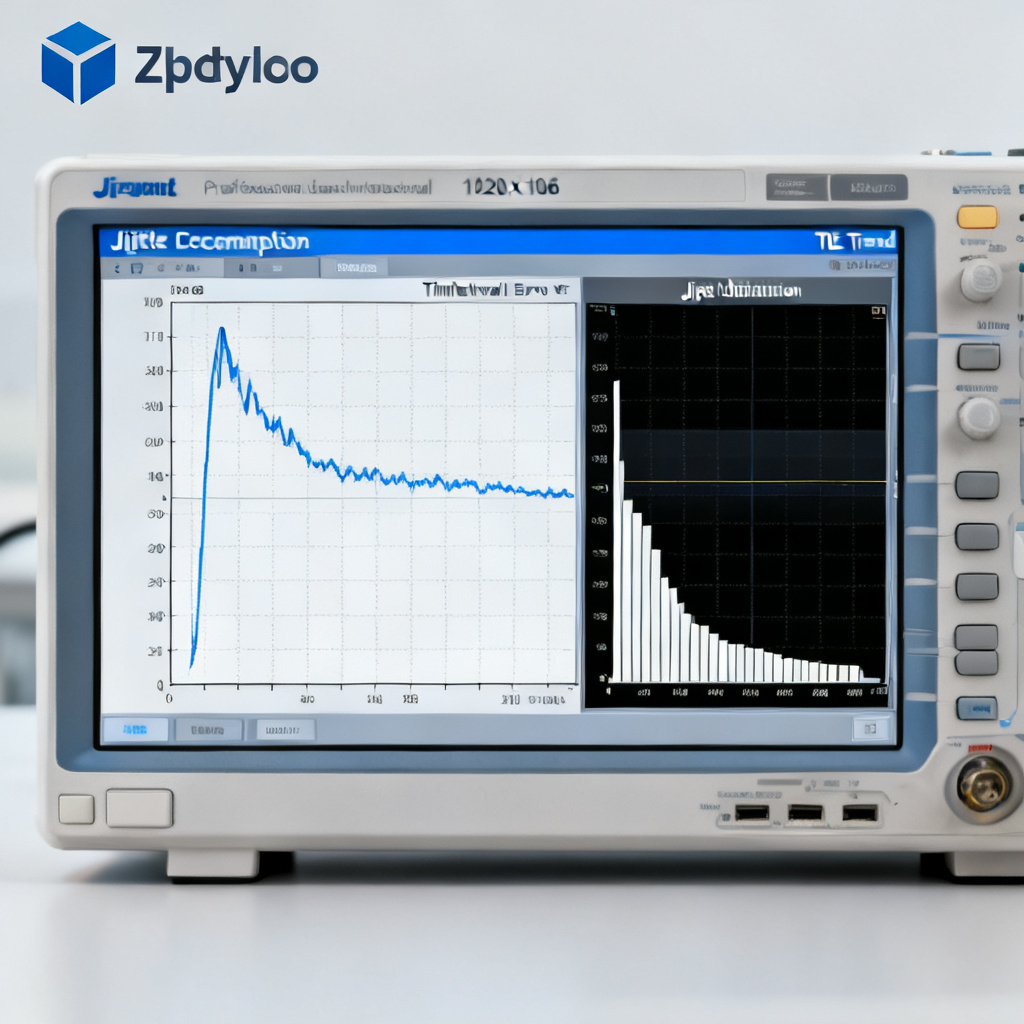
- Time Interval Error (TIE) Plot: The TIE plot will show a clear, repeating sinusoidal waveform over time.
Mitigation Strategies for Periodic Jitter
- Power Integrity (PI) Design: This is the #1 defense. Use a dedicated, low-noise voltage regulator module (VRM) for sensitive PLLs and clock buffers. Add extensive decoupling capacitors (bulk, ceramic, and high-frequency 0402/0201 caps) close to the power pins. Use power islands and proper stackup to create low-impedance power distribution networks (PDN).
- Shielding and Separation: Physically separate high-speed digital traces from clock lines and noisy power traces. Use ground guard traces around sensitive signals.
- Filtering: Add ferrite beads or low-pass filters on power supply lines entering sensitive analog or clock sections.
- Spread Spectrum Clocking (SSC): For systems where the periodic jitter is self-inflicted (e.g., from the reference clock), enabling SSC can spread the energy over a wider frequency band, reducing the peak jitter amplitude at any single frequency.
Measuring and Decomposing DJ: A Practical Guide
To effectively fix DJ, you must first measure it. Modern high-speed oscilloscopes and Bit Error Rate Testers (BERTs) offer powerful tools for jitter decomposition.
The Jitter Decomposition Process
- Acquire the Waveform: Use a real-time oscilloscope with sufficient bandwidth (e.g., 4x the data rate) and a high sampling rate. Capture a long record (millions of UI) to get good statistics.
- Extract the TIE: The instrument calculates the Time Interval Error for every clock edge, creating a TIE trend.
- Apply a Jitter Decomposition Algorithm: Software like Keysight’s N5391A Jitter Analysis or Tektronix’ DPOJET uses algorithms (e.g., the TailFit algorithm or Spectral Methods) to separate the total jitter histogram into Random Jitter (RJ) and Deterministic Jitter (DJ).
- Further Decompose DJ: Data-Dependent Jitter (DDJ) includes ISI. The algorithm correlates the TIE with the specific data pattern (e.g., using a PRBS pattern). DCD is detected by looking for a strong component at half the data rate. Pj is detected by identifying spectral peaks in the TIE spectrum.
Key Metrics to Report
- DJ(δδ): The peak-to-peak value of the deterministic jitter.
- RJ(rms): The RMS value of the random jitter.
- TJ(δδ) @ BER: The total jitter at a specific Bit Error Rate (e.g., 10^-12), typically calculated as TJ = DJ(δδ) + 14 * RJ(rms) (for BER=10^-12).
- Eye Height and Width: The voltage and time margins of the eye diagram.
Advanced Considerations and PCB Design Rules
The Interaction of DJ Types
In a real system, DJ types do not exist in isolation. A single imperfection can cause multiple DJ components. For example, a poorly designed via can cause a reflection (ISI) and also create a power supply disturbance (Pj). A driver with poor power supply rejection (PSR) will convert power supply ripple (Pj) into additional DCD. A holistic approach is required.
Stackup and Material Selection for DJ Reduction
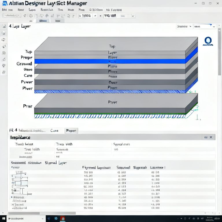
- Low-Loss Dielectrics: For high-speed serial links (e.g., 25 Gbps+), standard FR-4 is insufficient. Use materials like Megtron 6, Rogers 4000 series, or Isola Astra MT to minimize dielectric loss, which directly reduces ISI.
- Controlled Impedance: Tight tolerance on impedance (e.g., 50Ω ± 5%) is non-negotiable. This requires careful stackup design and manufacturing control.
- Return Path Integrity: Ensure a solid, continuous ground plane beneath every high-speed trace. Any gap in the return path creates an impedance discontinuity and introduces ISI and crosstalk.
The Role of the CDR (Clock and Data Recovery)
The CDR circuit in the receiver is the final line of defense. A well-designed CDR can track and filter out low-frequency Pj (e.g., from power supply noise) but cannot correct for high-frequency ISI or DCD. The CDR’s jitter tolerance specification defines how much DJ it can handle before failing. Your PCB design must ensure the DJ at the receiver input is below the CDR’s tolerance limit.
Comparison: Our High-Speed PCB Manufacturing Advantage
| Parameter | Standard PCB Manufacturer | Our High-Speed PCB Service |
|---|---|---|
| Impedance Tolerance | ±10% | ±5% (single-ended), ±10% (differential) |
| Material Options | FR-4 only | FR-4, Rogers, Megtron 6, Isola Astra MT |
| Via Processing | Standard via | Back-drilling, via-in-pad available |
| DJ Mitigation Support | Basic DFM | Advanced DFM review with jitter analysis guidance |
Frequently Asked Questions (FAQ)
What is Deterministic Jitter in high-speed PCB design?
Deterministic Jitter (DJ) is a bounded, predictable timing error in high-speed PCB signals, caused by specific sources like impedance mismatches, driver asymmetry, or power supply noise. It is distinct from random jitter and can be eliminated through proper design.
How does ISI affect my high-speed PCB?
Intersymbol Interference (ISI) occurs when previous data bits interfere with the current bit due to channel bandwidth limitations or impedance discontinuities. This Deterministic Jitter component reduces eye opening and increases bit error rates in your PCB.
Can DCD be fixed by PCB layout changes?
Duty Cycle Distortion (DCD) is primarily caused by driver asymmetry or threshold mismatch, which are often addressed at the component level. However, PCB layout can mitigate DCD by ensuring clean power delivery and minimizing DC offset through proper AC coupling.
What is the best way to measure Periodic Jitter in my PCB?
Use a real-time oscilloscope with jitter analysis software to capture the TIE trend and examine the jitter spectrum. Periodic Jitter appears as distinct spectral spurs, often from power supply noise or crosstalk, in your high-speed PCB measurements.
How can I reduce Deterministic Jitter in my next PCB prototype?
Focus on three key areas: use low-loss materials for the stackup, maintain tight impedance control (e.g., 50Ω ± 5%), and ensure a clean power distribution network. Our high-speed PCB manufacturing service provides advanced DFM review to help you minimize Deterministic Jitter.
Ready to eliminate jitter from your design? Contact our engineering team for a free DFM review and a quote on your next high-speed PCB prototype. We don’t just build boards; we build reliability.
Internal Links:
- How to Design a Low-Impedance Power Distribution Network
- High-Speed PCB Material Selection Guide: FR-4 vs. Rogers vs. Megtron
- Understanding Eye Diagrams for Signal Integrity
External References:
- Keysight Technologies: Jitter Analysis Fundamentals
- Tektronix: Jitter, Noise, and Signal Integrity Analysis
- IEEE P802.3bj Standard for 100GBASE-KR4 and 100GBASE-CR4