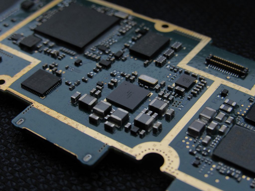
High-speed PCB troubleshooting is the core process to fix signal integrity, impedance, EMI, via, power integrity, timing, and manufacturing defects in 10Gbps–100Gbps circuit boards. This professional guide helps engineers and industrial buyers quickly locate failures and implement proven solutions.
High-Speed PCB Troubleshooting – Why Modern Boards Fail
Effective high-speed PCB troubleshooting starts with understanding failure root causes. Designs above 100MHz depend on stable impedance, complete return paths, low insertion loss, reasonable via structure, and consistent manufacturing quality.
Most failures are caused by impedance drift, discontinuous return paths, excessive high-frequency loss, poor via design, and process variation. These issues often combine to cause eye diagram closure, crosstalk, EMI failure, and intermittent communication errors. Unlike low-speed circuits, high-speed systems rely on precise transmission-line behavior, and even small deviations can lead to systemic signal collapse.
Common failure modes include impedance out of tolerance, differential pair mismatch, excessive crosstalk, signal reflection and ringing, high insertion loss, eye diagram closure, radiated and conducted EMI, via stub resonance, via impedance discontinuity, power supply noise, ground bounce, timing violations, random and deterministic jitter, open/short circuits, delamination, voids, and CAF growth. Each issue requires targeted diagnosis and standardized fixes.
Impedance Issues in High-Speed PCB Troubleshooting
Impedance errors are the most common problem in high-speed PCB troubleshooting. Standard controlled impedance includes 50Ω single-ended and 100Ω differential, which ensures stable transmission for PCIe, Ethernet, DDR, and USB4 interfaces.
Impedance Out of Tolerance
Symptoms: TDR test shows impedance out of ±10% tolerance, poor return loss, signal reflection, and higher bit error rate. Outer-layer microstrip traces are especially sensitive to process shifts.
Causes: Trace width etching error, dielectric thickness change, Dk value deviation, or incorrect stackup production.
Solutions: Verify Gerber dimensions against actual microsection measurements, require official impedance coupon test reports, audit production stackup for full compliance, and upgrade to ±5%–±7% tight-tolerance impedance control for critical channels.
Prevention: Reserve a ±15% design margin, confirm real material Dk/Df values before production, simulate impedance with factory process limits, and follow IPC-2221 guidelines.
Differential Pair Impedance Mismatch
Symptoms: 100Ω differential impedance deviation, large common-mode noise, increased EMI radiation, and unstable differential links such as HDMI, PCIe, and SFP28.
Causes: Unequal spacing between paired traces, intra-pair length mismatch, crossing reference plane gaps, and asymmetric via pad or anti-pad design.
Solutions: Standardize spacing across the entire pair, apply serpentine length compensation, add stitching vias at split planes, and unify via geometry for full electrical symmetry.
Prevention: Use rule-driven differential routing, place high-speed differential pairs on inner striplines, and avoid crossing plane splits.
Signal Integrity in High-Speed PCB Troubleshooting
Signal integrity problems dominate high-speed PCB troubleshooting because crosstalk, reflection, insertion loss, and eye diagram closure directly affect transmission reliability.
Excessive Crosstalk
Symptoms: Coupled noise spikes on adjacent traces, blurred eye diagrams, false triggering of sensitive signals, and failed NEXT/FEXT tests.
Causes: Violation of the 3W spacing rule, long parallel routing between high-speed clocks and sensitive lines, missing reference planes, and mixed placement of noisy and low-amplitude circuits.
Fixes: Enforce the 3W rule (center distance ≥ 3× trace width), add grounded guard traces with stitching vias, move critical high-speed signals to inner striplines, and break long parallel runs.
Prevention: Classify signals early, prioritize high-speed clock routing, and set automatic spacing constraints in EDA software.
Signal Reflection & Ringing
Symptoms: Overshoot/undershoot greater than 10% of signal swing, periodic ringing after edges, and setup/hold timing violations.
Causes: Impedance discontinuities at vias, connectors, or stubs; missing termination; long unused stubs; and multi-drop topology.
Fixes: Add 10–33Ω series termination near the driver, remove stubs using backdrilling, eliminate unused branch lines, and verify impedance continuity with TDR.
Prevention: Use point-to-point routing for signals above 100MHz and simulate impedance profiles before release.
Excessive Insertion Loss
Symptoms: Severe signal attenuation at the receiver, shrunken vertical eye opening, rapid decay of high-frequency components, and frame loss in long-distance transmission.
Causes: Overly long routes, high-Df lossy materials, rough copper increasing skin-effect loss, and excessive layer-changing vias.
Fixes: Shorten high-speed channel length, upgrade to low-loss materials such as Megtron 6 or Megtron 8, use HVLP ultra-smooth copper, and minimize via count.
Prevention: Complete channel loss budgeting during design and match materials to target data rate.
Eye Diagram Closure
Symptoms: Severe reduction in horizontal and vertical eye opening, heavy jitter, and failure of signal integrity compliance testing.
Causes: Combined effects of insertion loss, reflection, crosstalk, power noise, and common-mode EMI.
Fixes: Use high-speed oscilloscopes to decompose noise sources, optimize termination and vias to fix reflections, stabilize PDN to reduce jitter, and apply CTLE/DFE equalization at the receiver.
Prevention: Perform full-channel SI/PI simulation during design to ensure sufficient margin.
EMI & EMC in High-Speed PCB Troubleshooting
EMI certification failure is a key challenge in high-speed PCB troubleshooting. Most EMI issues come from broken return paths, common-mode current, and unshielded clock signals.
Radiated Emissions Failure
Symptoms: Sharp frequency spikes in EMI testing, unstable wireless modules, and failed FCC or CE certification.
Causes: High-speed traces crossing ground plane slots, common-mode current from unbalanced differential pairs, and unshielded clock harmonics.
Fixes: Eliminate cross-slot routing, add dense stitching vias, shield clock lines, and install common-mode chokes at connectors.
Prevention: Maintain continuous ground planes, minimize plane segmentation, and add filter locations at external ports.
Conducted Emissions & Susceptibility Issues
Symptoms: High-frequency noise on power rails, failed conducted emission tests, and poor immunity to external interference.
Causes: High PDN impedance, insufficient decoupling, and poorly placed capacitors.
Fixes: Deploy a full-band multi-value decoupling network, place capacitors extremely close to IC power pins, and add input filtering circuits.
Prevention: Simulate PDN impedance and meet target impedance goals for each power domain.
Via Problems in High-Speed PCB Troubleshooting
Via defects are critical for 10Gbps+ designs in high-speed PCB troubleshooting. Via stub resonance and impedance discontinuity are the top two via failures.
Via Stub Effect
Symptoms: Sharp notches in the insertion loss curve, sudden high-frequency attenuation, and increased bit error rates.
Causes: Unused via barrels creating resonant stubs; longer stubs resonate at lower frequencies.
Fixes: Apply backdrilling to remove excess stub length, use blind/buried vias, and limit residual stubs below 10mil.
Prevention: Make backdrilling default for 10Gbps+ designs and simulate stub resonance risk.
Via Impedance Discontinuity
Symptoms: TDR shows impedance dips at vias, increased local reflection, and degraded eye margin.
Causes: Parasitic capacitance from via pads, overly small anti-pads, and missing return vias.
Fixes: Enlarge anti-pads, reduce via pad size, and add nearby ground return vias.
Prevention: Use via simulation tools and enforce standardized high-speed via rules.
Power Integrity in High-Speed PCB Troubleshooting
Power integrity is often ignored but vital in high-speed PCB troubleshooting. Power noise, ripple, and ground bounce increase jitter and close eye diagrams.
Power Supply Noise & Ripple
Symptoms: Visible high-frequency ripple on power rails, unstable chip current, and increased signal jitter.
Causes: High PDN impedance, insufficient high-frequency decoupling, and loose power-ground coupling.
Fixes: Use multi-value capacitor banks, minimize capacitor loop inductance, and tightly couple power and ground layers.
Prevention: Design PDN using the target impedance method and validate with simulation.
Ground Bounce & SSO Noise
Symptoms: Sudden ground potential shifts during simultaneous switching, false logic levels, and unstable parallel buses.
Causes: High package and trace inductance, shared return paths, and insufficient ground pins.
Fixes: Increase ground pin and via count, partition high-speed I/O groups, and limit simultaneous switching.
Prevention: Separate noisy I/O sections and provide dedicated return paths.
Timing & Jitter Issues
Timing violation and excessive jitter cause data errors in DDR and parallel buses. Fix length matching, balance clock tree, and reduce simultaneous switching noise to improve timing margin.
Timing Violation & Setup-Hold Failure
Symptoms: Intermittent data errors in DDR or parallel buses, insufficient timing margin, and unstable performance at high temperature.
Causes: Severe length mismatch between data and clock lines, unbalanced clock tree, and excessive skew.
Fixes: Recalibrate route lengths, apply serpentine compensation, and optimize clock distribution.
Prevention: Enforce strict length-matching rules and reserve thermal margin.
Random Jitter & Deterministic Jitter
Symptoms: Compressed eye opening, rising bit error rates, and intermittent link drops.
Causes: Random jitter from thermal noise; deterministic jitter from crosstalk, reflection, EMI, and power noise.
Fixes: Use jitter decomposition to identify sources, eliminate deterministic interference, and improve thermal design.
Prevention: Implement holistic SI/PI/EMI design discipline.
Manufacturing Defects
Many high-speed failures come from manufacturing issues: open/short circuits, delamination, voids, and CAF. Follow IPC standards and DFM rules to reduce process risks.
Open & Short Circuits
Symptoms: Failed flying-probe or AOI tests, permanent open or short connections after assembly.
Causes: Over-etching, under-etching, drill shift, and residual copper.
Fixes: Review inspection reports, perform microsection analysis, and tighten factory process controls.
Prevention: Follow IPC DFM rules for minimum line width, spacing, and annular ring.
Delamination & Voids
Symptoms: Board bubbling, interlayer separation after reflow, and reduced insulation performance.
Causes: Moisture absorption, improper lamination, mismatched material Tg, and poor reflow profiles.
Fixes: Bake boards before assembly, optimize reflow temperature, and use high-Tg materials.
Prevention: Control storage humidity and follow IPC assembly guidelines.
CAF (Conductive Anodic Filament)
Symptoms: Falling insulation resistance, leakage current, and latent short circuits under high temperature and humidity.
Causes: Copper ion migration along glass fibers under voltage bias.
Fixes: Use CAF-resistant materials, increase clearance, and reduce sustained voltage bias.
Prevention: Follow IPC-9850 for high-reliability applications.
High-Speed PCB Troubleshooting Quick Reference Chart
| Symptom | Root Cause | First Check |
|---|---|---|
| Impedance out of tolerance | Trace width, Dk, dielectric variation | TDR report, stackup |
| Eye diagram closure | Loss + reflection + jitter | Termination, via stubs, PDN |
| Excessive crosstalk | Spacing too small, long parallel runs | 3W rule, guard traces |
| EMI failure | Return path broken, common-mode current | Cross-slot routing, stitching vias |
| Frequency notch | Via stub resonance | Backdrilling, stub length |
| DDR timing error | Length mismatch, clock skew | Length calibration, clock tree |
| Power ripple | Poor decoupling, high PDN impedance | Cap placement, power-ground coupling |
| Open/short | Etch/drill error | AOI, flying probe, microsection |
Core Takeaways for High-Speed PCB Troubleshooting
All high-speed PCB troubleshooting returns to four core points: impedance continuity, complete return paths, controlled high-frequency loss, and stable power distribution network.
Effective debugging follows a consistent cycle: identify symptoms → locate root causes → apply proven fixes → implement long-term prevention. Pre-production SI/PI simulation eliminates more than 80% of high-speed risks before manufacturing. Combining IPC-compliant design, rigorous DFM review, appropriate high-speed material selection, and expert manufacturing partnership ensures reliable mass production and minimal failure rates.
FAQ About High-Speed PCB Troubleshooting
What is the most important step in high-speed PCB troubleshooting?
The most important step in high-speed PCB troubleshooting is checking impedance control and return path integrity, which cause over 60% of signal failures.
How do you fix eye diagram closure in high-speed PCB troubleshooting?
In high-speed PCB troubleshooting, fix eye closure by improving termination, removing via stubs, stabilizing power integrity, and reducing crosstalk and insertion loss.
What materials help most in high-speed PCB troubleshooting?
Low-Df high-speed materials like Megtron 6/8 and HVLP copper are most effective in high-speed PCB troubleshooting to reduce loss and improve signal quality.
Why is EMI common in high-speed PCB troubleshooting?
EMI is common in high-speed PCB troubleshooting due to broken return paths, common-mode current, and unshielded high-speed clock signals.
Which IPC standards support high-speed PCB troubleshooting?
IPC-2221, IPC-6012, IPC-9121, and IPC-9850 provide critical standards for impedance, reliability, and defect resolution in high-speed PCB troubleshooting.
Get Professional High-Speed PCB Troubleshooting Support
If you need expert help with high-speed PCB troubleshooting, our engineering team provides free design review, TDR testing, failure analysis, DFM optimization, and custom high-speed PCB manufacturing for global industrial clients.
We support 10G, 25G, 56G, and 100G high-speed applications for industrial, automotive, medical, and data center products. Submit your Gerber files or test reports to receive a free professional review and quotation. We help you resolve failures quickly, pass EMC and SI certification, and launch stable, production-ready designs on time.