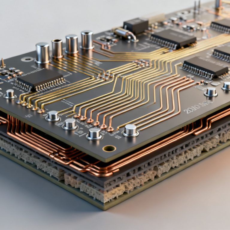
Measuring jitter in high speed PCB designs is critical for ensuring signal integrity at multi-gigabit data rates. This guide explains how to use a Real Time Oscilloscope to accurately capture and analyze timing deviations, enabling engineers to diagnose and resolve jitter-related failures in advanced digital systems.
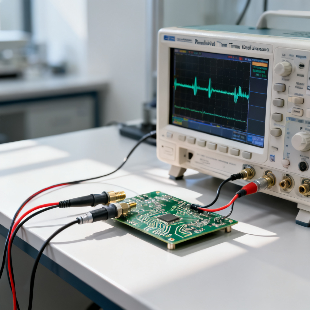
1. Understanding Jitter – The Foundation of Measurement for Jitter in High Speed PCB
Before connecting probes, it is essential to understand what jitter is and why it matters in the context of jitter in high speed PCB analysis.
1.1 What is Jitter?
Jitter is defined as the deviation of a signal’s timing from its ideal or expected position. In a perfect digital system, clock edges and data transitions occur at precise, equally spaced intervals. In reality, due to noise, crosstalk, power supply fluctuations, and material imperfections, these transitions occur slightly earlier or later than expected.
Mathematically, jitter is often expressed as:
- Time Interval Error (TIE): The difference between the actual edge position and the ideal edge position.
- Peak-to-Peak Jitter (Jpp): The total range of timing variation.
- RMS Jitter (Jrms): The standard deviation of the timing variation.
1.2 Why Jitter Matters in High-Speed PCBs
At high speeds (e.g., 10 Gbps, 25 Gbps, or higher), the timing margin for data sampling shrinks dramatically. A small amount of jitter in high speed PCB can:
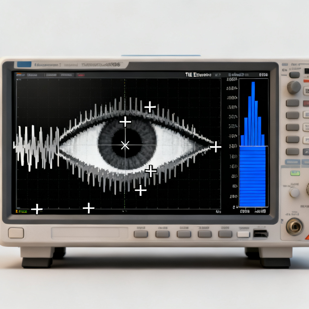
- Reduce the eye diagram opening: Causing the eye to close, making it harder for the receiver to distinguish a 0 from a 1.
- Increase Bit Error Rate (BER): Directly causing data transmission failures.
- Cause system lock-up: In clock recovery circuits, excessive jitter can cause the Phase-Locked Loop (PLL) to lose lock.
1.3 Types of Jitter: Deterministic vs. Random
To measure jitter effectively, you must separate its components. Jitter is generally classified into two main categories:
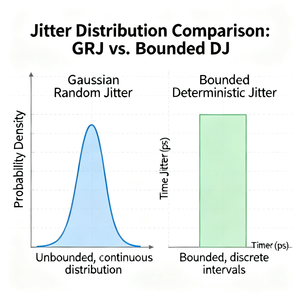
- Random Jitter (RJ):
- Source: Inherently random processes such as thermal noise, shot noise, and flicker noise.
- Characteristics: Unbounded, Gaussian distribution. It has no pattern and cannot be predicted.
- Measurement: Typically measured as RMS value (1 sigma). The peak-to-peak value grows with measurement time.
- Deterministic Jitter (DJ):
- Source: System-specific, repeatable causes such as crosstalk, power supply noise, impedance mismatches, and data-dependent effects.
- Characteristics: Bounded, non-Gaussian distribution. It has a finite peak-to-peak value.
- Sub-categories:
- Periodic Jitter (PJ): Caused by switching power supplies, clock harmonics, or other repetitive noise sources. Appears as spurs in the frequency domain.
- Data-Dependent Jitter (DDJ): Caused by inter-symbol interference (ISI) due to bandwidth limitations or reflections.
- Duty Cycle Distortion (DCD): Caused by asymmetric rise/fall times or threshold offsets.
2. The Real-Time Oscilloscope – Your Primary Tool for Jitter in High Speed PCB Measurement
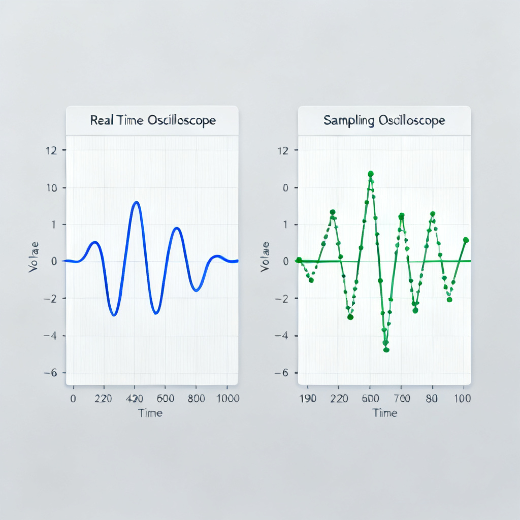
A Real-Time Oscilloscope (RTO) is the most common and versatile instrument for jitter in high speed PCB analysis. Unlike a sampling oscilloscope, an RTO captures a continuous waveform in a single acquisition, allowing you to see the actual waveform behavior, including non-repetitive events.
2.1 Key Oscilloscope Requirements
To measure jitter in high speed PCB accurately, your RTO must meet these minimum specifications:
| Parameter | Requirement for Jitter in High Speed PCB | Explanation |
|---|---|---|
| Bandwidth | 3 to 5 times the fundamental frequency | For a 10 Gbps signal (5 GHz fundamental), a 25 GHz to 33 GHz oscilloscope is recommended. Lower bandwidth will filter the signal and artificially reduce the measured jitter. |
| Sample Rate | 2.5 to 4 times the bandwidth | For a 33 GHz scope, a sample rate of 100 GS/s or more is typical. Higher sample rates provide better timing resolution. |
| Low Internal Jitter Floor | At least 10x lower than the jitter to be measured | The oscilloscope itself introduces jitter. You must ensure that the scope’s own jitter floor (typically specified as RMS jitter) is significantly lower than the DUT’s jitter. |
| Deep Memory | 1 Gpts or more | Jitter analysis often requires capturing millions of bits to get statistically significant results. Deep memory is essential for long acquisition windows. |
| Specialized Jitter Analysis Software | Keysight N883xA, Tektronix DPOJET, LeCroy SDA | These packages automate TIE extraction, jitter separation, and eye diagram analysis. |
2.2 Why Use a Real-Time Oscilloscope (vs. Sampling Scope)?
| Feature | Real-Time Oscilloscope (RTO) | Sampling Oscilloscope |
|---|---|---|
| Acquisition | Captures the entire waveform in one trigger event. | Reconstructs waveform by sampling over many repetitions. |
| Single-shot events | Can capture and analyze non-repetitive jitter events. | Cannot capture single-shot events. |
| Time-correlated analysis | Allows you to see jitter in the context of the entire signal. | Provides statistical jitter only. |
| Bandwidth | Typically lower (up to 110 GHz currently). | Can achieve very high bandwidth (up to 100+ GHz). |
| Best for | Debugging, troubleshooting, system-level jitter analysis. | High-frequency, repetitive signal characterization. |
Conclusion: For comprehensive jitter in high speed PCB measurement in a real-world environment where you need to see the actual waveform, RTO is the preferred tool.
3. Step-by-Step Measurement Procedure for Jitter in High Speed PCB
This section details the exact steps to measure jitter in high speed PCB using a Real-Time Oscilloscope.
Step 1: Setup and Calibration
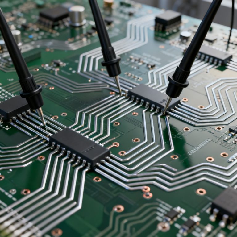
Probe Selection and Connection:
- Use high-impedance active probes (e.g., 1 MΩ) for low-speed signals or 50 Ω SMA cables for high-speed differential signals.
- Impedance Matching: Ensure the probe’s input impedance matches the characteristic impedance of the PCB trace (typically 50 Ω single-ended, 100 Ω differential). Use a 50 Ω feed-through termination if measuring a high-speed signal with a 1 MΩ probe.
- Probe Loading: Minimize probe loading. A 0.5 pF probe capacitance is acceptable for most applications. For ultra-high-speed signals, consider using a differential probe with a very low input capacitance.
- Grounding: Use the shortest possible ground lead (ideally a ground spring or direct tip-to-ground connection) to avoid creating a ground loop that adds noise and jitter.
Oscilloscope Calibration:
- Perform deskew between channels if measuring differential signals. This ensures that the two channels have identical time delays.
- Self-calibration: Run the oscilloscope’s internal self-calibration routine to compensate for temperature and drift.
Vertical and Horizontal Settings:
- Vertical Scale: Set the vertical scale so that the signal fills approximately 80% of the screen to maximize the dynamic range of the ADC.
- Timebase (Horizontal Scale): Set the timebase to capture at least 1 million UI (Unit Intervals). For a 10 Gbps signal, this means a time window of 100 µs. This is critical for capturing low-frequency jitter components.
- Triggering: Use an edge trigger on the clock signal or a pattern trigger on a known data pattern (like a PRBS31) to start the acquisition.
Step 2: Acquiring the Waveform
Number of Acquisitions: Acquire multiple waveforms (e.g., 100 to 1000) to build a statistically significant dataset. The more acquisitions, the more accurate the jitter histogram.
Persistent Display: Enable infinite persistence to visually see the jitter accumulation over time. You will see the waveform edges become fuzzy or thick, indicating the presence of jitter.
Eye Diagram Mode: Most RTOs have an eye diagram mode. This is the most intuitive way to see jitter. The eye pattern is created by overlaying many UI transitions. A wide, open eye indicates low jitter; a narrow, closed eye indicates high jitter.
Step 3: Extracting TIE (Time Interval Error)
TIE is the raw data from which all jitter metrics are derived.
Select the Clock Recovery Method: You must define the ideal clock against which jitter is measured.
- PLL-based Clock Recovery: Simulates the behavior of a receiver’s PLL. You must set the PLL bandwidth (e.g., 10 MHz, 100 MHz) according to your system standard. This is the most realistic method for system-level testing.
- Constant Clock: Uses a fixed, ideal clock frequency. This is simpler but may overestimate jitter because it does not account for the PLL’s ability to track low-frequency wander.
Define the Threshold Level: Set the voltage threshold (typically 50% of the signal amplitude) at which the oscilloscope measures the crossing time.
Extract TIE: The oscilloscope software will calculate the time difference between each actual edge crossing and the ideal clock edge. This TIE vector is the foundation for all subsequent analysis.
Step 4: Jitter Analysis and Separation
Now, use the oscilloscope’s jitter analysis software to decompose the total jitter.
Total Jitter (TJ): This is the overall jitter. It is often specified at a specific BER (e.g., TJ @ BER 1e-12).
Jitter Histogram: Plot the TIE values as a histogram.
- The shape of the histogram reveals the jitter type:
- Gaussian-like shape: Indicates dominant Random Jitter (RJ).
- Bimodal or multi-peak shape: Indicates Deterministic Jitter (DJ), especially DCD or PJ.
- Wide, flat distribution: Suggests ISI or data-dependent jitter.
Jitter Spectrum (Phase Noise Plot): Perform an FFT on the TIE data to create a jitter spectrum.
- Spurs at specific frequencies: Indicate Periodic Jitter (PJ). Identify the frequency of the spur to trace the noise source (e.g., a 100 MHz switching regulator).
- High noise floor: Indicates high Random Jitter (RJ).
Bathtub Curve: Plot the BER as a function of the sampling point. The “bathtub” shape shows how the BER increases as you move away from the center of the eye. The width of the bathtub at a given BER (e.g., 1e-12) is the Total Jitter (TJ).
Jitter Separation (Dual-Dirac Method):
- The most common method to separate RJ and DJ.
- The software fits two Gaussian curves to the tails of the jitter histogram.
- DJ (δδ): The distance between the means of the two Gaussians.
- RJ (σ): The standard deviation of the Gaussian tails.
- TJ = DJ + 2 * σ * BER_factor (e.g., for BER 1e-12, the factor is approximately 14.069).
Step 5: Interpreting Results
- If RJ is dominant: The issue is likely noise-related (power supply, ground bounce, thermal noise). Focus on improving power integrity, shielding, and layout.
- If DJ is dominant: The issue is deterministic. Examine the jitter spectrum to find the frequency of the spur (PJ) or analyze the data pattern to identify ISI (DDJ). This often points to impedance discontinuities, crosstalk, or poor termination.
- If DCD is high: Check the rise/fall time symmetry of your driver and the threshold voltage of your receiver.
4. Common Pitfalls and Best Practices for Jitter in High Speed PCB Measurement
Even with the best equipment, incorrect measurement techniques can lead to flawed results when measuring jitter in high speed PCB.
4.1 Pitfall: Insufficient Measurement Time
- Problem: Jitter, especially random jitter, is unbounded. A short measurement (e.g., 1,000 UI) will underestimate the peak-to-peak jitter.
- Solution: Always measure over a long time window (millions of UI). Use the oscilloscope’s deep memory and long persistence mode to capture low-frequency wander and rare events.
4.2 Pitfall: Incorrect Clock Recovery Settings
- Problem: Using a PLL bandwidth that is too high or too low compared to your system’s receiver can give misleading results. A high PLL bandwidth will track out low-frequency jitter, making the signal look better than it is.
- Solution: Always use the PLL bandwidth specified by the relevant standard (e.g., PCIe, USB, Ethernet). If no standard exists, choose a bandwidth that matches your receiver’s PLL characteristics.
4.3 Pitfall: Probe Loading and Grounding
- Problem: A long ground lead (e.g., a 3-inch ground wire) acts as an inductor, creating a resonant circuit that adds noise and jitter. A probe with excessive capacitance can also load the signal, changing its shape.
- Solution: Use the shortest possible ground connection (spring tip) and a low-capacitance probe. Always verify that the probe is not distorting the signal.
4.4 Pitfall: Ignoring the Oscilloscope’s Own Jitter
- Problem: The oscilloscope’s internal jitter floor adds to your measurement. If the scope’s jitter is comparable to the DUT’s jitter, your results will be inaccurate.
- Solution: Measure the oscilloscope’s jitter floor by shorting the input and measuring the jitter on the noise. Ensure the DUT’s jitter is at least 10x higher than the floor. If not, use a lower-jitter scope or apply de-embedding techniques.
4.5 Best Practice: Use a PRBS Pattern
- Recommendation: For data-dependent jitter (DDJ) analysis, always use a Pseudo-Random Binary Sequence (PRBS) pattern (e.g., PRBS7, PRBS15, PRBS31). A PRBS pattern contains all possible bit sequences, which will excite all sources of ISI and DCD. A simple clock pattern (1010) will not reveal ISI.
4.6 Best Practice: Correlate with Simulation
- Recommendation: Before going to the lab, simulate your PCB’s signal integrity using tools like HyperLynx, ADS, or SIwave. Compare the simulated jitter (especially DJ from ISI) with your measured results. A large discrepancy indicates a problem in your simulation model or your measurement setup.
5. Advanced Techniques and Troubleshooting for Jitter in High Speed PCB
For complex jitter in high speed PCB problems, advanced methods are needed.
5.1 Separating ISI from Other DJ Components
- ISI (Inter-Symbol Interference): Caused by bandwidth limitations. It is pattern-dependent. To measure ISI, use a Bit Error Rate Tester (BERT) in conjunction with the oscilloscope, or use the oscilloscope’s pattern lock feature to isolate the jitter on specific bit sequences (e.g., “0001” vs. “1110”).
- Crosstalk-Induced Jitter: Caused by aggressor signals. To isolate it, turn off the aggressors one by one and observe the change in the jitter spectrum.
5.2 Using the Oscilloscope for Time-Domain Reflectometry (TDR)
- Application: If you suspect impedance mismatches are causing DDJ, use the oscilloscope’s TDR mode (if available) or a separate TDR to measure the impedance profile of the PCB trace. A sudden impedance change (e.g., from 50 Ω to 60 Ω) will cause reflections and jitter.
5.3 De-embedding and Fixture Removal
- Problem: Your measurement fixture (cables, connectors, probes) adds its own jitter and signal degradation.
- Solution: Use the oscilloscope’s de-embedding feature to mathematically remove the effects of the fixture from the measurement. This requires a model (S-parameters) of the fixture.
5.4 Troubleshooting with the Jitter Spectrum
- Example: If you see a strong spur at 100 MHz in the jitter spectrum, it is highly likely that a 100 MHz switching regulator or a 100 MHz clock harmonic is coupling into your signal path.
- Action: Check the power supply decoupling near the driver, improve the shielding, or reroute the clock trace away from the data trace.
Conclusion
Measuring jitter in high speed PCB using a Real-Time Oscilloscope is a multi-faceted process that requires a solid understanding of jitter types, proper instrument setup, and careful interpretation of results. By following the step-by-step procedure outlined here—from probe selection and clock recovery to jitter separation and spectrum analysis—you can accurately diagnose and resolve timing issues in your designs.
Remember these key takeaways:
- Use a high-bandwidth, low-jitter RTO with deep memory.
- Always extract TIE and use it to build histograms and jitter spectra.
- Separate RJ from DJ to identify the root cause.
- Avoid common pitfalls like insufficient measurement time and poor probe grounding.
- Correlate your measurements with simulations and system-level requirements.
By mastering these techniques, you ensure that your high-speed PCBs operate reliably at the edge of performance, minimizing bit errors and maximizing system robustness.
Need a high-speed PCB with guaranteed low jitter performance? Contact our engineering team today for a free signal integrity consultation and a custom quote.
FAQ
What is the most common method to measure jitter in high speed PCB?
The most common method is using a Real Time Oscilloscope with TIE extraction and the Dual-Dirac jitter separation technique. This approach allows engineers to quantify both Random Jitter and Deterministic Jitter components accurately.
How does oscilloscope bandwidth affect jitter in high speed PCB measurement?
Insufficient bandwidth filters out high-frequency content, artificially reducing the measured jitter. For reliable jitter in high speed PCB analysis, the oscilloscope bandwidth should be at least 3 to 5 times the fundamental signal frequency.
Can I measure jitter in high speed PCB without a clock recovery PLL?
Yes, but using a constant clock reference may overestimate jitter because it does not simulate the receiver’s ability to track low-frequency wander. For system-level accuracy, always use a PLL-based clock recovery with the correct bandwidth.
What is the difference between TIE and peak-to-peak jitter in high speed PCB?
TIE (Time Interval Error) is the raw timing deviation of each edge from the ideal clock. Peak-to-peak jitter is the range of all TIE values. TIE is the foundation for all advanced jitter analysis, while peak-to-peak gives a simple total variation metric.
Why is probe grounding critical for jitter in high speed PCB measurement?
A long ground lead creates inductance that adds noise and false jitter. Using a spring tip or direct ground connection minimizes this effect, ensuring the measured jitter in high speed PCB is from the DUT, not the probe.