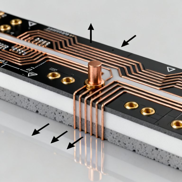
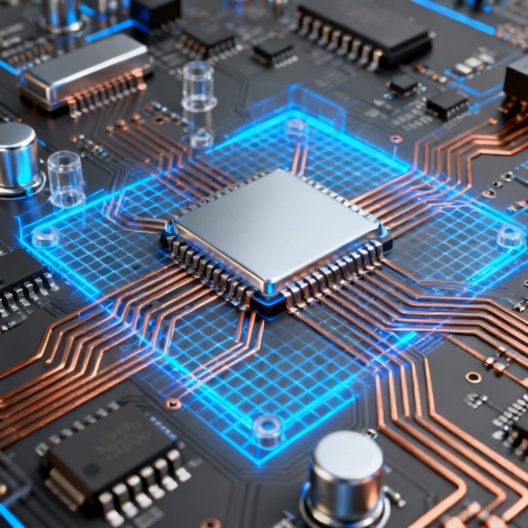
In high-speed PCB design, modal crosstalk in high speed PCB—specifically common mode to differential mode conversion—is a critical signal integrity challenge. This mechanism degrades differential signaling performance by converting unwanted common-mode noise into differential-mode errors. Understanding this conversion is essential for engineers designing boards for 10 Gbps+ SerDes, DDR5, or PCIe Gen 5/6.
Fundamentals of Modal Crosstalk in High Speed PCB
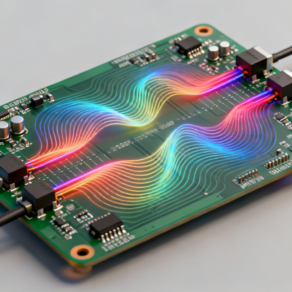
Modal crosstalk in high speed PCB occurs when a common-mode signal on an aggressor differential pair couples asymmetrically to a victim differential pair. Unlike conventional crosstalk, this exploits the modal structure of transmission lines. Differential signaling relies on two complementary traces (D+ and D-) carrying equal but opposite voltages. Ideally, external noise couples equally to both traces and cancels out. Common-mode noise arises from switching noise, crosstalk from adjacent nets, return path discontinuities, and skew or asymmetry within the pair.
Physics of Common Mode to Differential Mode Conversion
Modal Decomposition of Differential Pairs
A differential pair supports two propagation modes: differential mode (odd mode) where signals are 180° out of phase, and common mode (even mode) where signals are in phase. In an ideal symmetric pair, these modes are orthogonal. However, asymmetries cause common mode to differential mode conversion. When a common-mode wave encounters an asymmetry, part of its energy transfers to the differential mode.
The Conversion Mechanism
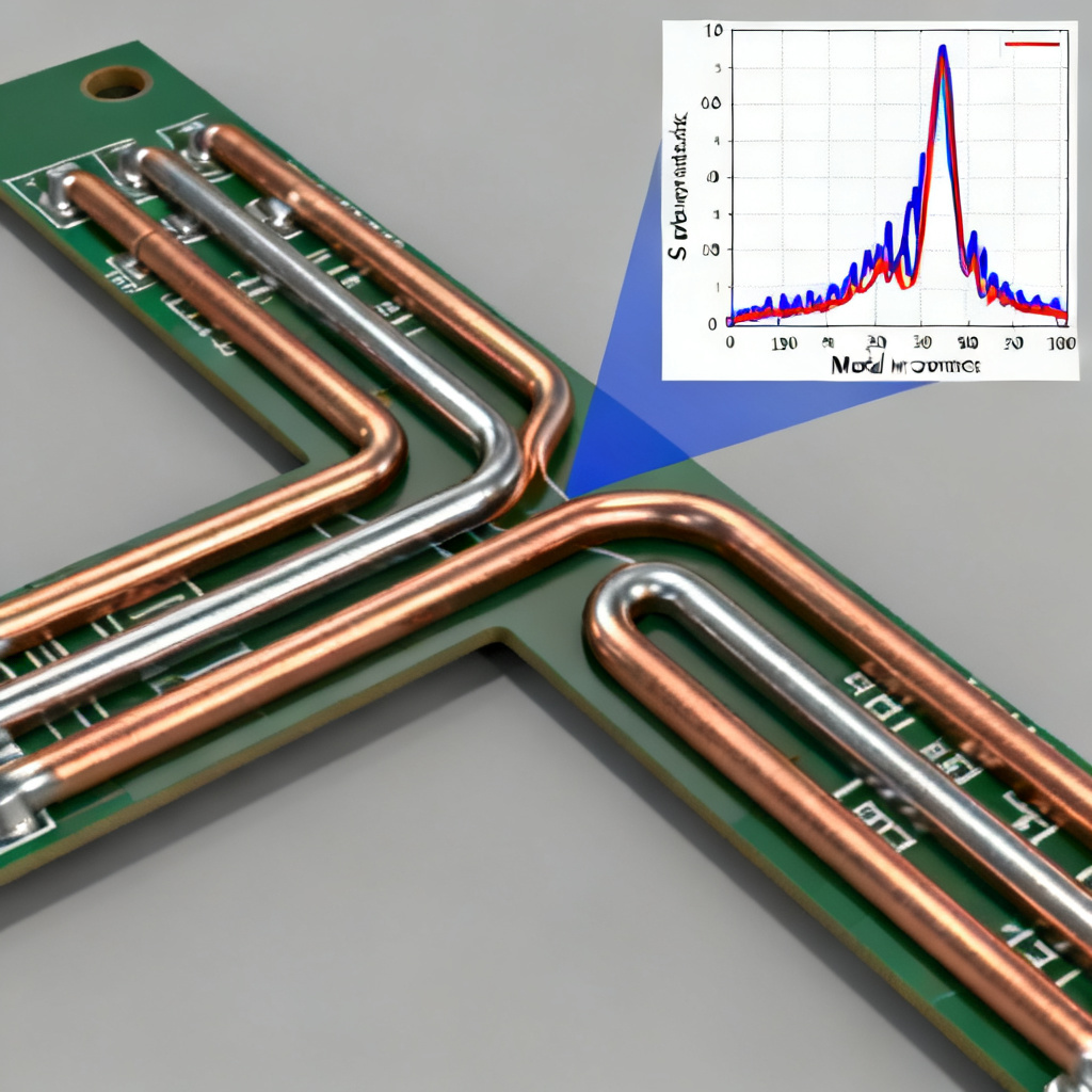
Consider an aggressor differential pair carrying a common-mode signal. If the victim pair has geometric or impedance asymmetry, the coupling coefficients differ. This imbalance converts a portion of the aggressor’s common-mode field into a differential-mode voltage. The conversion efficiency is quantified by S_CD21 (common-mode to differential-mode conversion). A typical acceptable limit is below -40 dB for high-speed digital links.
Sources of Modal Crosstalk in High Speed PCB
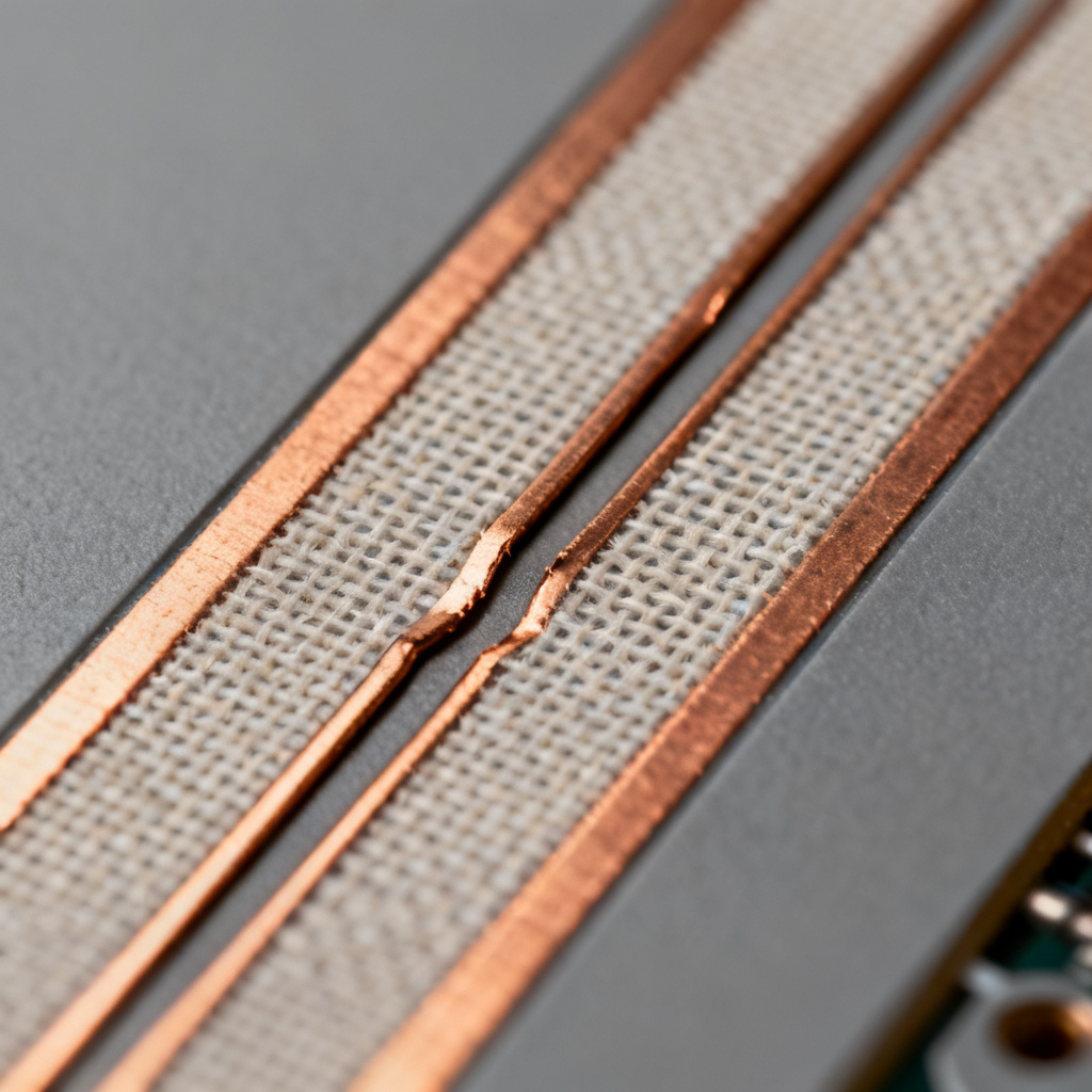
Asymmetric Trace Geometry
Width or trace thickness variation, spacing variation, and dielectric anisotropy (e.g., FR4 fiber weave orientation) cause impedance mismatch and mode conversion. For high speed PCB designs, even 0.5 mil differences can degrade performance.
Discontinuities in the Return Path
Split reference planes and via transitions force return currents to detour, inducing common-mode noise and asymmetry. Differential via pairs with unequal stubs or antipad sizes create conversion points.
Skew and Length Mismatch
Intra-pair skew of just 5 ps can cause significant mode conversion at 10+ GHz. The common-mode component couples differently due to the time offset.
Proximity to Other Aggressors
Broadside or edge coupling between layers creates imbalance. This is especially problematic in stripline configurations.
Modeling and Simulation of Modal Crosstalk in High Speed PCB
Engineers use full-wave EM simulators (e.g., Ansys HFSS, Keysight ADS) to predict modal crosstalk. Steps include creating a 3D model, defining differential and common-mode ports, running S-parameter simulation, analyzing S_CD21, and identifying dominant coupling paths. A simulation of a 6-layer board shows that a 10-mil length mismatch increases S_CD21 from -45 dB to -28 dB at 5 GHz.
| Parameter | Value (Ideal) | Value (With Mismatch) |
|---|---|---|
| Differential Impedance | 100 ohms | 95 ohms |
| Intra-Pair Skew | 0 ps | 5 ps |
| S_CD21 at 5 GHz | -45 dB | -28 dB |
| Eye Opening | 90% | 70% |
Design Rules to Minimize Modal Crosstalk in High Speed PCB
Maintain Symmetry Within Each Differential Pair
Match trace width, thickness, and spacing to within ±0.5 mil. Keep intra-pair skew below 2 ps. Use low-loss, homogeneous materials like Rogers or Megtron 6.
Optimize Return Path Continuity
Avoid split planes. If crossing is unavoidable, use stitching capacitors. Use back-drilled vias and symmetric antipads.
Manage Aggressor-Victim Coupling
Increase center-to-center spacing to at least 3× dielectric height (H). Use guard traces stitched with vias. Prefer stripline over microstrip for inner layers.
Terminate Common-Mode Noise
Use common-mode chokes or ferrite beads on the receiver side. Use AC coupling capacitors matched in value and placement.
Validate with Post-Layout Simulation
Run mixed-mode S-parameter simulation targeting S_CD21 < -40 dB up to Nyquist frequency.
Case Study: Modal Crosstalk in High Speed PCB (16-Layer Board)
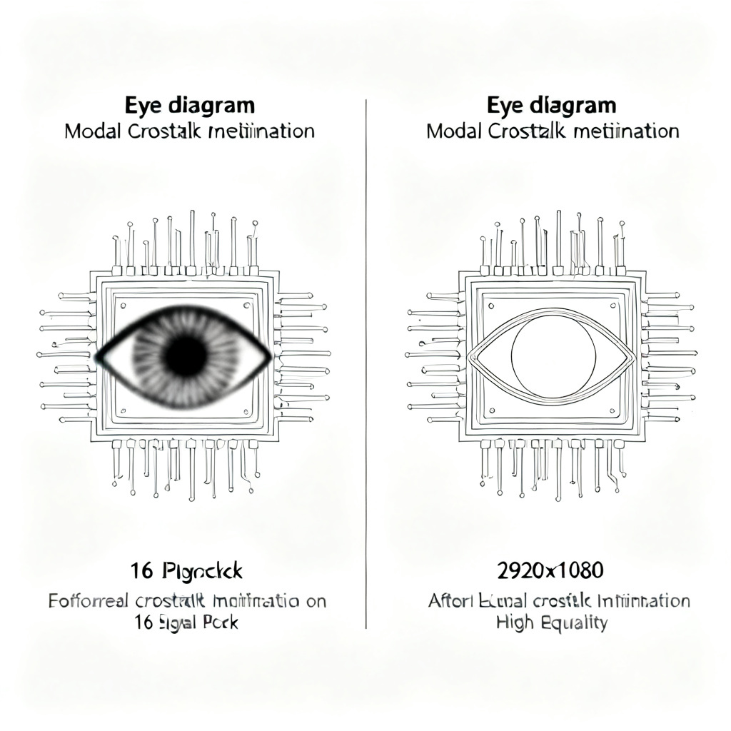
A 16-layer PCB for 10 Gbps Ethernet and PCIe Gen 4 exhibited bit errors. Simulation revealed modal crosstalk between adjacent differential pairs on Layer 4. The victim pair had a 3-mil width mismatch, and the aggressor carried strong common-mode noise. S_CD21 peaked at -32 dB at 2.5 GHz. Mitigation included adjusting victim pair width tolerance, adding a common-mode choke, and increasing pair spacing from 15 mil to 25 mil. S_CD21 dropped to -48 dB, and the eye diagram opened fully.
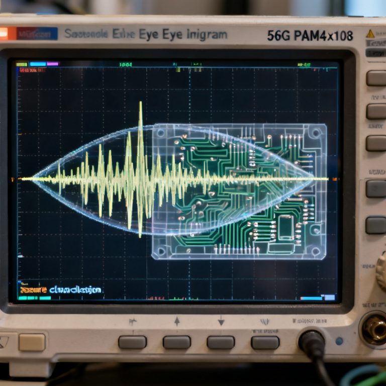
Testing and Verification for Modal Crosstalk in High Speed PCB
Verification methods include TDR, frequency-domain S-parameter measurement with a VNA, and eye diagram analysis. Acceptance criteria per IPC-2141A and JEDEC: differential impedance tolerance ±10%, intra-pair skew < 5 ps, mode conversion < -35 dB for 1-10 GHz.
FAQ: Modal Crosstalk in High Speed PCB
- What is modal crosstalk in high speed PCB?
- Modal crosstalk in high speed PCB refers to the conversion of common-mode noise into differential-mode signals due to asymmetries in differential pairs.
- How does common mode to differential mode conversion affect signal integrity?
- Common mode to differential mode conversion creates parasitic differential signals that bypass the receiver’s common-mode rejection, causing jitter and bit errors.
- What are the main causes of modal crosstalk in high speed PCB?
- Main causes include asymmetric trace geometry, return path discontinuities, intra-pair skew, and proximity to other aggressor pairs.
- How can I minimize modal crosstalk in high speed PCB design?
- Maintain symmetry, ensure return path continuity, increase spacing, use common-mode chokes, and validate with post-layout simulation.
- What is an acceptable S_CD21 value for high speed PCB?
- An S_CD21 below -40 dB is acceptable for most high-speed digital links; below -30 dB often indicates a problem.
Industry Terminology for Modal Crosstalk in High Speed PCB
Differential impedance: The impedance seen by a differential signal, typically 100 ohms. Common-mode rejection ratio (CMRR): A measure of a differential receiver’s ability to reject common-mode signals. Mode conversion: The transfer of energy between common and differential modes, quantified by S_CD21. Intra-pair skew: The time delay difference between the two traces of a differential pair.
Comparison: Our High Speed PCB vs. Standard Manufacturing
| Feature | Our High Speed PCB | Standard PCB |
|---|---|---|
| Trace Width Tolerance | ±0.3 mil | ±0.5 mil |
| Intra-Pair Skew Limit | < 2 ps | < 5 ps |
| Mode Conversion (S_CD21) | < -45 dB | < -35 dB |
| Material Options | Rogers, Megtron 6 | FR4 |
| Post-Layout Simulation | Included | Not included |
Ready to Build High Speed PCBs with Minimal Modal Crosstalk?
Contact our engineering team for a free DFM review and stackup optimization tailored to your next project. We specialize in modal crosstalk in high speed PCB mitigation, ensuring first-pass success for 10 Gbps+ designs.