Understanding jitter in High Speed PCB for PCIe 5.0 compliance is essential for any engineer designing 32 GT/s links. With a unit interval of only 31.25 picoseconds, the timing margin is extremely tight. If jitter exceeds the budget, the receiver’s clock and data recovery circuit fails, causing bit errors and system instability.
1. The PCIe 5.0 Jitter Budget: Deconstructing the Limits for High Speed PCB
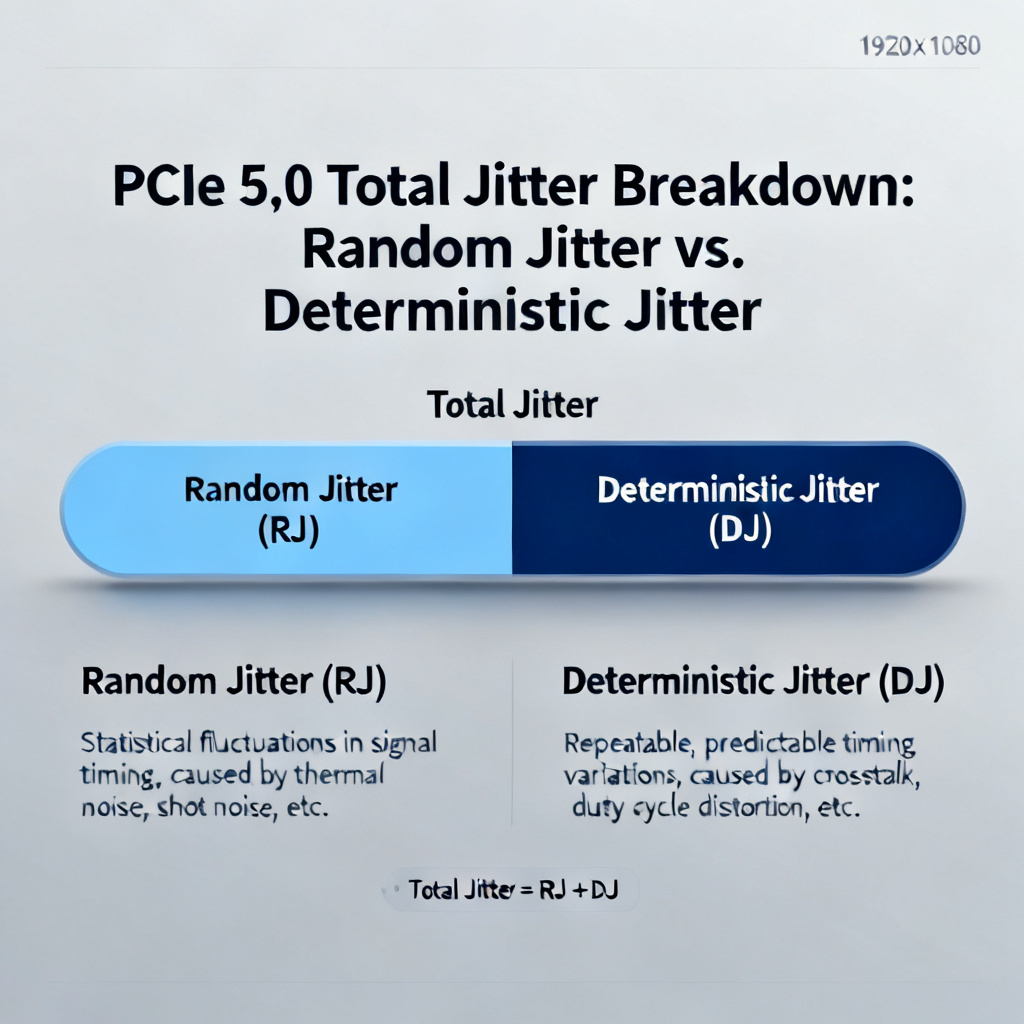
For any High Speed PCB targeting PCIe 5.0, the jitter budget is defined by the PCI-SIG Base Specification. The budget is split into Random Jitter (Rj) and Deterministic Jitter (Dj), calculated using the Dual-Dirac model at a BER of 1e-12.
1.1 Core Budget Equation for PCIe 5.0 High Speed PCB
Total Jitter (Tj) at the receiver input is typically 0.5 UI (15.6 ps). The channel (PCB + connector) budget is only 0.15–0.2 UI (4.7–6.25 ps). This is the primary limit for jitter in High Speed PCB for PCIe 5.0 compliance.
1.2 Key Jitter Components and Limits in High Speed PCB
Rj (thermal noise) is negligible in the PCB itself but significant in silicon. Dj is the main concern for PCB designers, broken into four sub-components:
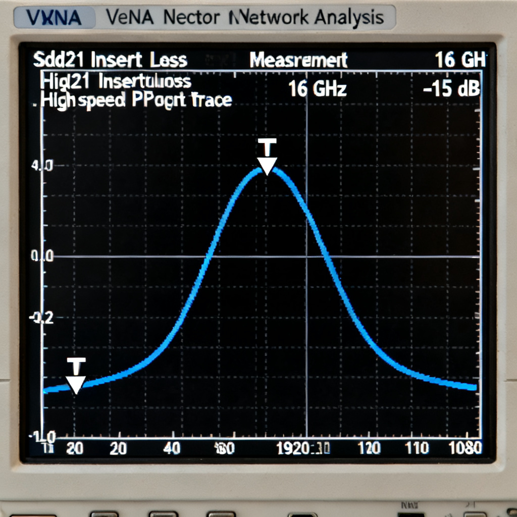
- Data-Dependent Jitter (DDJ): Caused by ISI from loss. The insertion loss at 16 GHz must be less than -20 dB to -25 dB.
- Duty Cycle Distortion (DCD): From asymmetric edges. Limit is typically <2 ps.
- Periodic Jitter (PJ): From power supply noise or clock coupling. Must be kept below a few ps.
- Bounded Uncorrelated Jitter (BUJ): From crosstalk. Single-ended crosstalk must be <-35 dB at 16 GHz.
2. The Three Pillars of PCIe 5.0 Jitter Control in High Speed PCB
Three physical mechanisms generate jitter in a High Speed PCB: loss, crosstalk, and impedance discontinuities. Each has a strict limit.
2.1 Pillar 1: Managing Insertion Loss (DDJ Limit) for High Speed PCB
Loss at 16 GHz creates ISI, the dominant source of DDJ. The limit for the PCB trace alone is -10 dB to -15 dB at 16 GHz. Use low-loss laminates like Megtron 6 or Rogers 3000 series (Df <0.005), VLP copper, and back-drilled vias with stubs <10 mils.
2.2 Pillar 2: Controlling Crosstalk (BUJ Limit) in High Speed PCB
Crosstalk from adjacent lanes injects BUJ. The limit is -35 dB for single-ended crosstalk at 16 GHz. Use 4W–5W spacing, guard traces, tightly coupled differential pairs, and ground vias near signal vias.
2.3 Pillar 3: Eliminating Impedance Discontinuities in High Speed PCB
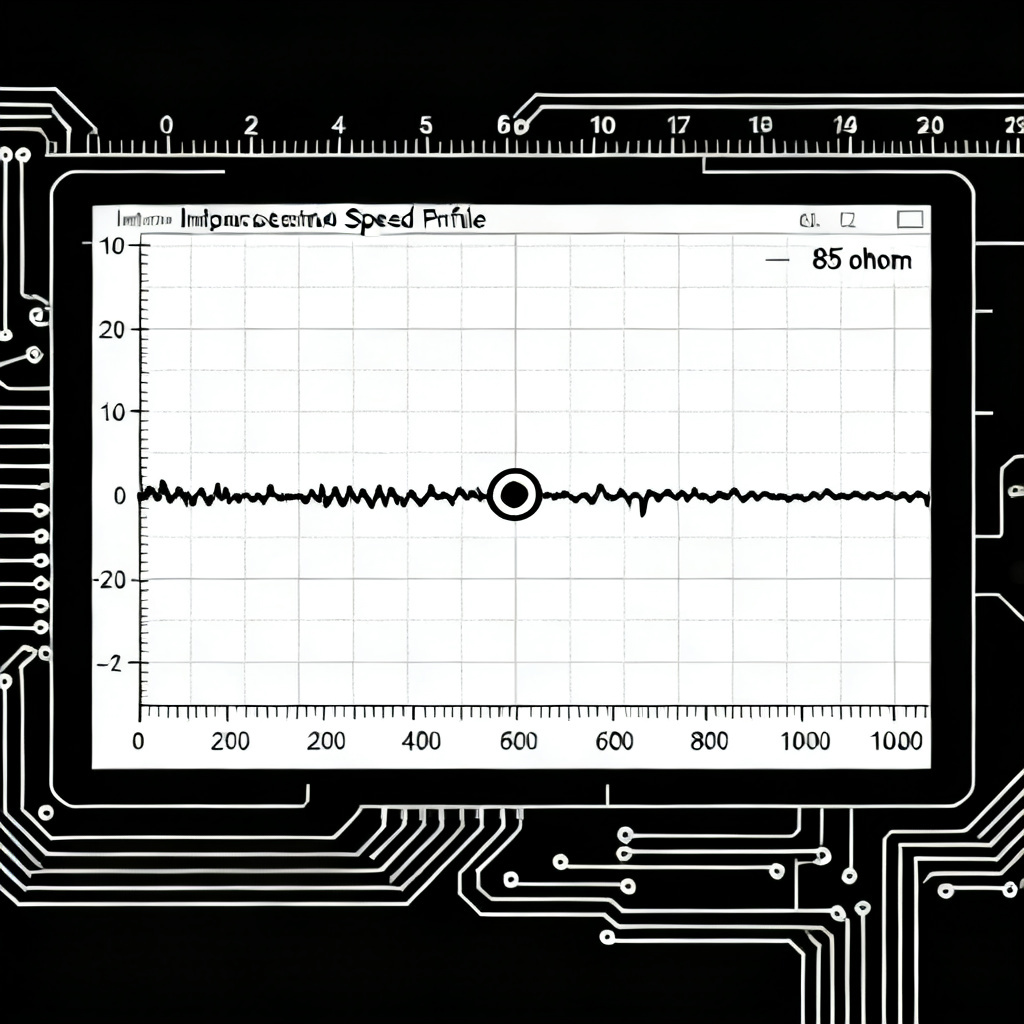
Impedance mismatches cause reflections that shift zero-crossings. The differential impedance must be 85 ohms ±10%. Return loss (Sdd11) must be better than -10 dB at 16 GHz. Use precise trace geometry, optimized via anti-pads, and necking down at connector breakouts.
3. PCIe 5.0 Compliance Test & Simulation Limits for High Speed PCB
To guarantee jitter in High Speed PCB for PCIe 5.0 compliance, simulation and measurement are mandatory.
3.1 Pre-Layout Simulation Limits
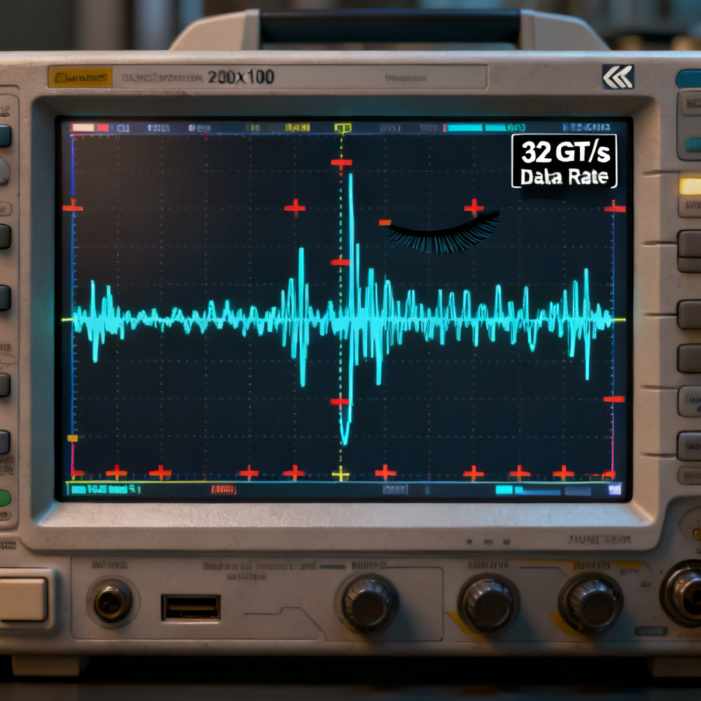
Channel Operating Margin (COM) must be >3 dB. The eye diagram must show minimum eye height of 20 mV and eye width of 0.3 UI (9.4 ps).
3.2 Post-Layout Measurement Limits
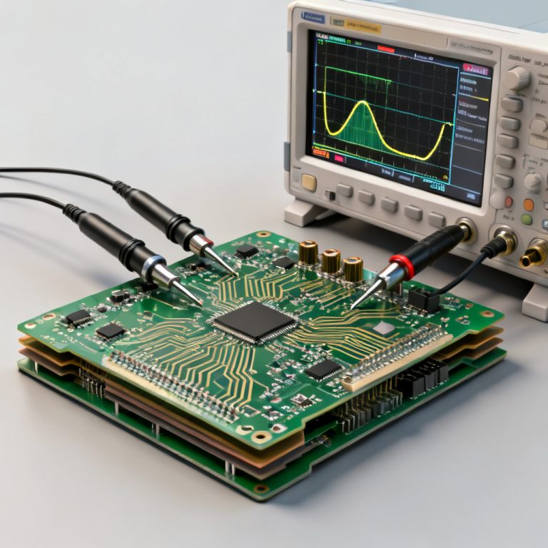
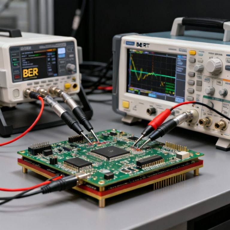
TDR must show no impedance discontinuities greater than ±10%. S-parameters must show Sdd21 within loss budget and Sdd11 below -10 dB. Measured Tj must be less than 0.5 UI.
4. Practical PCB Design Limits for PCIe 5.0 High Speed PCB
Here is a structured table of the key limits for jitter in High Speed PCB for PCIe 5.0 compliance:
| Parameter | Limit for PCIe 5.0 High Speed PCB | Why It Matters |
|---|---|---|
| Dielectric Material Df | <0.005 at 10 GHz | Controls DDJ from loss |
| Copper Foil | VLP or RTF | Reduces skin effect loss |
| Differential Impedance | 85 ohms ±10% | Prevents reflections & DCD |
| Trace Length | <10–12 inches (low-loss material) | Exceeding causes excessive DDJ |
| Via Stub Length | <10 mils (back-drill) | Prevents resonant loss |
| Crosstalk (NEXT/FEXT) | <-35 dB at 16 GHz | Prevents BUJ |
| Return Loss (Sdd11) | <-10 dB at 16 GHz | Prevents reflection jitter |
| Insertion Loss (Sdd21) | <-15 dB at 16 GHz (PCB trace only) | Primary DDJ control |
| Channel Operating Margin | >3 dB | Ensures overall link health |
| Total Jitter at Rx | <0.5 UI (15.6 ps) | Must be met for BER 1e-12 |
5. Conclusion: Path to PCIe 5.0 High Speed PCB Compliance
Jitter in High Speed PCB for PCIe 5.0 compliance is a system-level challenge. A 1 dB increase in loss or a 5% impedance mismatch can push the system over the edge. For a PCB manufacturer, the path is clear: select low Df materials with VLP copper, design for 85 ohms ±10%, back-drill all vias, simulate for COM >3 dB, and measure TDR, S-parameters, and eye diagrams. Ignoring these limits results in link failures and costly redesigns.
Ready to build a High Speed PCB that meets PCIe 5.0 compliance? Contact our engineering team for a free stack-up review and simulation. We specialize in low-jitter manufacturing for high-speed serial links.
FAQ: Jitter in High Speed PCB for PCIe 5.0 Compliance
What is the total jitter budget for PCIe 5.0 High Speed PCB?
The total jitter (Tj) at the receiver input is 0.5 UI (15.6 ps) at a BER of 1e-12. The channel budget is 0.15–0.2 UI (4.7–6.25 ps).
How does crosstalk affect jitter in High Speed PCB for PCIe 5.0?
Crosstalk generates Bounded Uncorrelated Jitter (BUJ). Single-ended crosstalk must be kept below -35 dB at 16 GHz to stay within the jitter budget.
What materials are best for minimizing jitter in High Speed PCB?
Use low-loss laminates like Megtron 6, Megtron 7, or Rogers 3000/4000 series with a dissipation factor (Df) below 0.005 at 10 GHz. VLP copper foil is also essential.
What is Channel Operating Margin (COM) for PCIe 5.0?
COM is a comprehensive metric that includes all jitter sources. For PCIe 5.0 compliance, COM must be greater than 3 dB. This ensures the link can tolerate the specified jitter.
Why is impedance control critical for jitter in High Speed PCB?
Impedance mismatches cause reflections that shift zero-crossings, creating deterministic jitter. The differential impedance must be 85 ohms ±10% to prevent this.