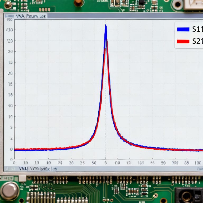
Understanding why an eye diagram PCB collapse occurs is critical for high-speed digital design. The primary drivers are noise and vertical closure, which reduce signal margins and increase bit error rates. This guide explores the root causes, from crosstalk to impedance mismatches, and provides actionable mitigation strategies for B2B PCB manufacturers.
Understanding the Eye Diagram and Vertical Closure in Eye Diagram PCB Collapse
What Is an Eye Diagram?
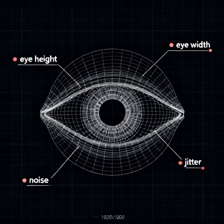
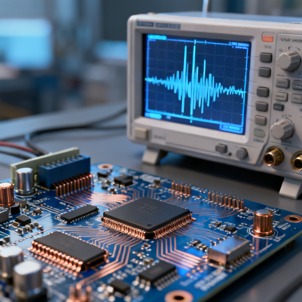
An eye diagram is created by overlaying multiple transitions of a digital signal (e.g., from 0 to 1, 1 to 0) on an oscilloscope. Key metrics include:
- Eye Height: The vertical opening, indicating noise margin.
- Eye Width: The horizontal opening, indicating timing margin.
- Jitter: Timing variations that narrow the eye horizontally.
- Rise/Fall Times: Speed of transitions, affecting the eye’s shape.
Vertical Closure Defined in Eye Diagram PCB Collapse
Vertical closure refers to the reduction in eye height due to noise and signal degradation. When noise pushes the signal closer to the decision threshold, the eye collapses vertically, making it harder for the receiver to distinguish a 1 from a 0.
Why Vertical Closure Matters for Eye Diagram PCB Collapse
A closed eye directly increases the bit error rate (BER). For high-speed PCBs (e.g., PCIe Gen 4/5, USB 3.2, 10GbE), a small vertical margin can lead to intermittent failures. In B2B manufacturing, this translates to costly field returns and reduced reliability.
Noise as a Primary Cause of Eye Diagram PCB Collapse
Types of Noise Affecting the Eye in Eye Diagram PCB Collapse
Noise is the most common cause of vertical closure. It introduces random or deterministic voltage fluctuations that compress the eye. The three main types are:
- Thermal Noise (Johnson-Nyquist): Inherent in resistors and conductive traces. It is broadband and random, reducing signal-to-noise ratio (SNR).
- Shot Noise: Caused by current flow across junctions (e.g., in active components). It is frequency-dependent and more pronounced at high speeds.
- Flicker Noise (1/f Noise): Dominant at low frequencies but can modulate high-speed signals via power supply ripple.
Crosstalk: The Dominant Noise Source in PCB Layout for Eye Diagram PCB Collapse
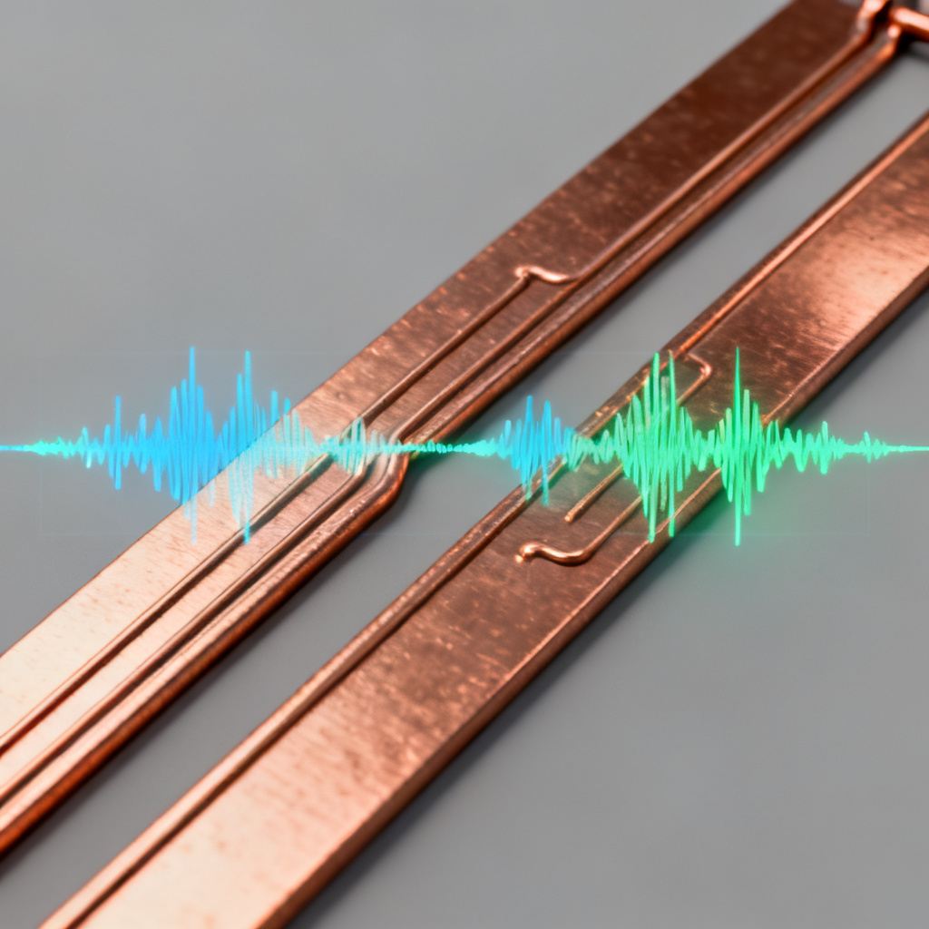
Crosstalk is electromagnetic interference between adjacent traces. It is a deterministic noise source that directly reduces eye height. Key mechanisms:
- Capacitive Coupling: Occurs when two traces run parallel for long distances. The faster the edge rate, the stronger the coupling.
- Inductive Coupling: Caused by mutual inductance in return paths. It is worse in poorly referenced planes.
- Far-End Crosstalk (FEXT): Travels in the same direction as the aggressor signal, adding to the victim’s noise.
- Near-End Crosstalk (NEXT): Travels backward, affecting signals on the same layer.
Impact on Eye Diagram: Crosstalk adds a voltage spike or dip at the sampling point, reducing the vertical opening. In dense high-speed designs, crosstalk can shrink the eye by 30-50%.
Power Supply Noise (PSN) and Eye Diagram PCB Collapse
PSN arises from switching currents in the power delivery network (PDN). It modulates the reference voltage for drivers and receivers, creating a DC offset that shifts the eye vertically. Sources include:
- Simultaneous switching noise (SSN) from multiple outputs.
- Poor decoupling capacitor placement.
- Insufficient plane capacitance.
Impact: PSN increases the noise floor, lowering the eye’s top and raising its bottom. This is a common cause of vertical closure in multi-layer PCBs.
Reflections and Impedance Mismatches Contributing to Eye Diagram PCB Collapse
When a signal encounters an impedance discontinuity (e.g., via stub, connector, or trace width change), part of the energy is reflected back. These reflections create overshoot, undershoot, and ringing that distort the eye vertically.
- Overshoot: Pushes the signal above the nominal high level, but can also cause false triggering.
- Undershoot: Dips below the low level, reducing the eye bottom.
- Ringing: Oscillations that add noise to the sampling window.
Vertical Closure Mechanisms That Collapse the Eye in Eye Diagram PCB Collapse
Attenuation and Skin Effect in Eye Diagram PCB Collapse
At high frequencies (e.g., 10GHz+), the skin effect forces current to flow on the conductor surface, increasing resistance and signal loss. Dielectric loss in the PCB substrate (e.g., FR-4 vs. low-loss materials) further attenuates high-frequency components. This reduces the amplitude of transitions, directly shrinking the eye vertically.
- Dielectric Loss Tangent: Materials like FR-4 have high loss at 10GHz, causing 1-2dB/inch attenuation. Low-loss laminates (e.g., Rogers, Isola) preserve amplitude.
- Insertion Loss: Measured in dB, it quantifies how much the signal weakens over the trace length. A loss of 3dB halves the voltage swing.
Jitter and Its Effect on Vertical Closure in Eye Diagram PCB Collapse
Jitter is primarily a horizontal issue, but it indirectly causes vertical closure. When jitter shifts the sampling point, the receiver captures the signal at a non-optimal time, where the voltage is lower. This is known as vertical jitter-induced closure.
- Random Jitter (RJ): Gaussian distribution, caused by thermal noise. It widens the distribution of sampling times.
- Deterministic Jitter (DJ): Includes crosstalk, ISI, and power supply noise. It creates specific patterns that align with data transitions.
Mechanism: At the eye’s center, the voltage is highest. But if jitter pushes the sampling instant to the edge of the eye, the voltage drops. This effect is amplified by slow rise/fall times.
Inter-Symbol Interference (ISI) and Eye Diagram PCB Collapse
ISI occurs when the channel’s bandwidth is insufficient to pass the highest frequency components of the data stream. This causes the signal to “ring” from one bit to the next, creating a pattern-dependent DC offset.
- Example: A long string of 1s followed by a single 0 can cause the 0 to appear higher than the actual low level, collapsing the eye bottom.
- Impact: ISI is a major cause of vertical closure in long PCB traces (e.g., >10 inches).
Return Path Discontinuities and Eye Diagram PCB Collapse
A broken or high-impedance return path (e.g., a gap in the ground plane, or a via transition without a ground via) forces the signal to find a longer return path. This creates a voltage drop across the plane, adding noise and reducing the eye height.
- Via Stubs: Unused via stubs act as transmission line stubs, creating resonances that attenuate specific frequencies.
- Split Planes: Crossing a split plane (e.g., analog and digital grounds) introduces a large inductive loop, causing vertical closure.
How to Diagnose and Measure Vertical Closure in Eye Diagram PCB Collapse
Using an Oscilloscope with Eye Diagram Analysis
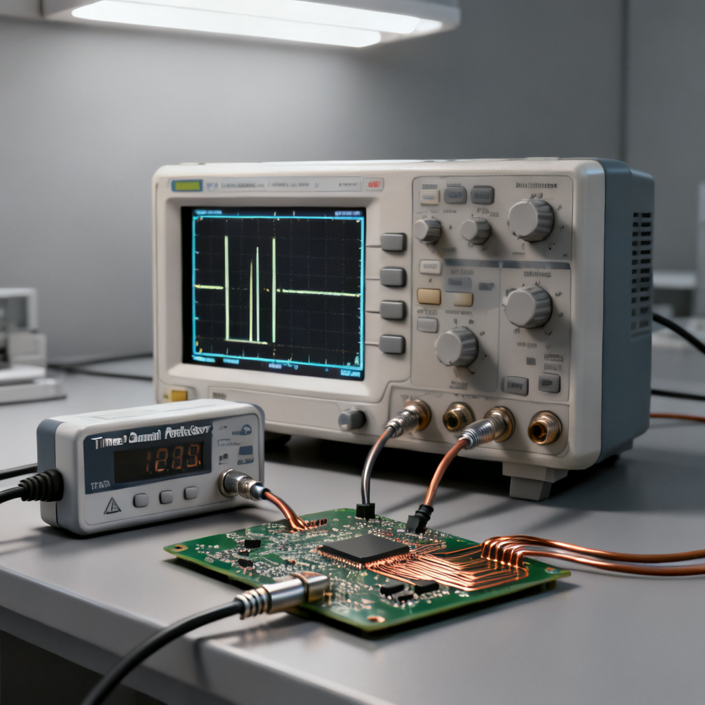
- Setup: Use a high-bandwidth scope (4x the data rate) and a clock recovery unit.
- Measurement: Measure the eye height at the 50% crossing point. Compare to the nominal swing (e.g., 800mV for LVDS). A drop of >20% indicates a problem.
- Bathtub Curve: Plot BER vs. sampling point to see vertical margin.
Simulation Tools for Pre-Production
- SI Simulation (e.g., HyperLynx, Ansys SIwave): Predict eye height based on stackup, trace geometry, and material properties.
- Statistical Analysis: Use IBIS-AMI models to simulate jitter and noise contributions.
- TDR (Time Domain Reflectometry): Locate impedance discontinuities that cause reflections.
Key Metrics to Monitor
- Eye Height (mV): Target >200mV for 1V differential signals.
- Eye Width (ps): Target >70% of the unit interval (UI).
- Noise Margin: The difference between the noise floor and the signal level.
- BER Floor: The minimum achievable BER; a high floor indicates vertical closure.
Mitigation Strategies for High-Speed PCB Design to Prevent Eye Diagram PCB Collapse
Layout Techniques to Reduce Noise
- Controlled Impedance: Match trace impedance to the driver and receiver (e.g., 50Ω single-ended, 100Ω differential). Use impedance calculators for your stackup.
- Differential Pair Routing: Keep pairs tightly coupled (e.g., 5-10 mil spacing) and at equal length to reject common-mode noise.
- Guard Traces: Place grounded traces between aggressor and victim lines to reduce crosstalk.
- Minimize Stubs: Use back-drilling to remove via stubs in high-speed traces.
Material and Stackup Choices
- Low-Loss Dielectrics: Use Rogers 4350B, Isola I-Tera, or Megtron 6 for 10Gbps+ designs. Avoid FR-4 above 5Gbps.
- Thinner Dielectrics: Reduce layer-to-layer spacing to lower crosstalk.
- Multiple Ground Planes: Use at least two dedicated ground planes for signal return.
Power Integrity Solutions
- Decoupling Capacitors: Place 0.1μF and 0.01μF caps near each IC, with low-inductance vias.
- Power Plane Design: Use a solid copper plane for VCC and ground. Avoid slots or splits.
- Ferrite Beads: Filter high-frequency noise on power rails.
Signal Conditioning
- Pre-Emphasis/De-Emphasis: Boost the first transition to compensate for loss.
- Equalization: Use CTLE (Continuous Time Linear Equalizer) or DFE (Decision Feedback Equalizer) in the receiver.
- Re-drivers/Re-timers: For long traces, add active repeaters to restore signal amplitude.
Testing and Validation
- Eye Mask Testing: Ensure the eye passes the mask defined by standards (e.g., PCIe, USB).
- BER Testing: Run a PRBS (Pseudo-Random Bit Sequence) pattern for 10^12 bits to verify BER.
- Temperature and Voltage Sweep: Test at worst-case conditions to ensure margin.
Real-World Case Studies of Eye Diagram PCB Collapse
Case Study 1: 10GbE Backplane with 20-inch Traces
A client’s backplane showed 40% eye height reduction. Root cause: FR-4 material with high dielectric loss and poor return path due to a split ground plane. Solution: Switched to Isola I-Tera, added a solid ground plane, and used back-drilling. Eye height improved from 150mV to 350mV.
Case Study 2: PCIe Gen 4 with Crosstalk
Two PCIe lanes on adjacent layers showed 50% eye closure. Root cause: 15-mil spacing with no guard trace. Solution: Increased spacing to 25 mils and added a grounded copper pour between lanes. Eye height recovered to 90% of nominal.
FAQ: Eye Diagram PCB Collapse
What is the main cause of eye diagram PCB collapse?
The main cause of eye diagram PCB collapse is noise, including crosstalk, power supply noise, and reflections, which lead to vertical closure by reducing the eye height and margin.
How does crosstalk contribute to eye diagram PCB collapse?
Crosstalk introduces deterministic voltage spikes or dips at the sampling point, directly reducing the vertical opening of the eye diagram. This is a key factor in eye diagram PCB collapse in dense high-speed designs.
What is vertical closure in an eye diagram?
Vertical closure refers to the reduction in eye height due to noise and signal degradation. It is a primary symptom of eye diagram PCB collapse, making it harder for receivers to distinguish logic levels.
How can I prevent eye diagram PCB collapse in my design?
To prevent eye diagram PCB collapse, use controlled impedance, low-loss materials, proper decoupling, guard traces, and signal conditioning techniques like equalization and pre-emphasis.
What tools are used to diagnose eye diagram PCB collapse?
Oscilloscopes with eye diagram analysis, SI simulation tools (e.g., HyperLynx, Ansys SIwave), and TDR are commonly used to measure eye height, jitter, and identify causes of eye diagram PCB collapse.
Comparison of Noise Sources in Eye Diagram PCB Collapse
| Noise Source | Effect on Eye Diagram PCB Collapse | Mitigation Strategy |
|---|---|---|
| Crosstalk | Reduces eye height by 30-50% | Increase trace spacing, use guard traces |
| Power Supply Noise | Shifts DC offset, lowers noise margin | Add decoupling capacitors, solid planes |
| Reflections | Causes overshoot/undershoot | Match impedance, minimize stubs |
| Jitter | Indirectly reduces vertical margin | Use low-jitter clocks, equalization |
Glossary of Terms for Eye Diagram PCB Collapse
- Eye Diagram: An oscilloscope display of a digital signal’s transitions, used to assess signal quality.
- Vertical Closure: The reduction in eye height due to noise, a key indicator of eye diagram PCB collapse.
- Crosstalk: Unwanted electromagnetic coupling between adjacent traces.
- Jitter: Timing variations in signal transitions.
- Inter-Symbol Interference (ISI): Distortion caused by insufficient channel bandwidth.
- Return Path Discontinuity: A break in the signal’s ground return path, causing noise.