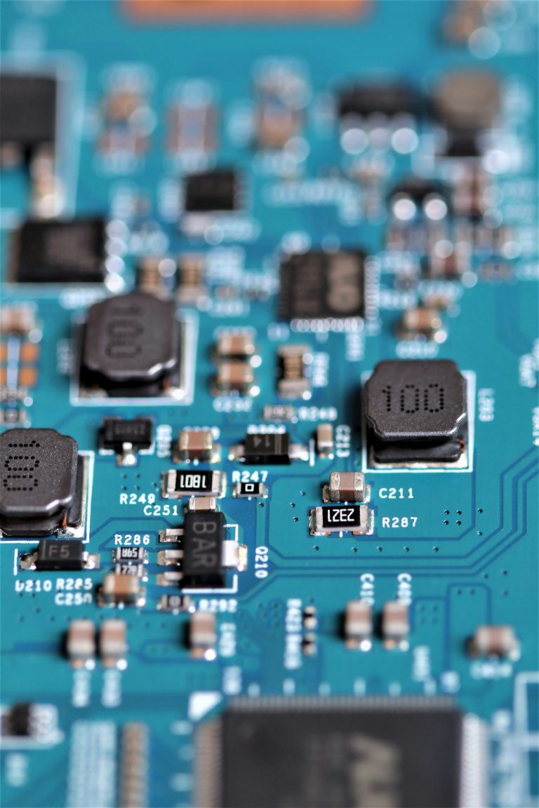
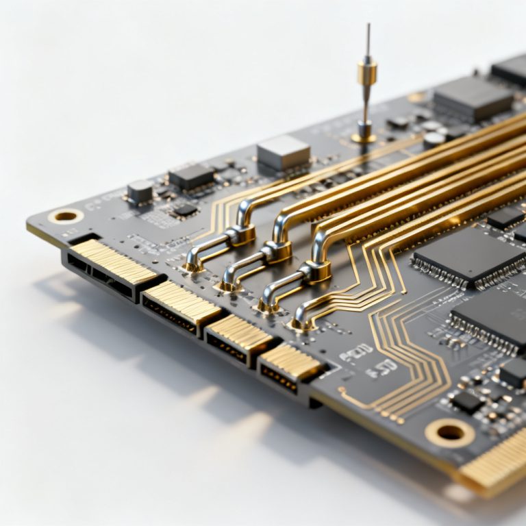
Periodic jitter in high speed PCB designs is a critical signal integrity challenge, often originating from the switching noise of power supplies. This timing error degrades system performance and must be understood and mitigated for reliable high-speed operation. We explore the root causes, measurement techniques, and design solutions for this pervasive issue.
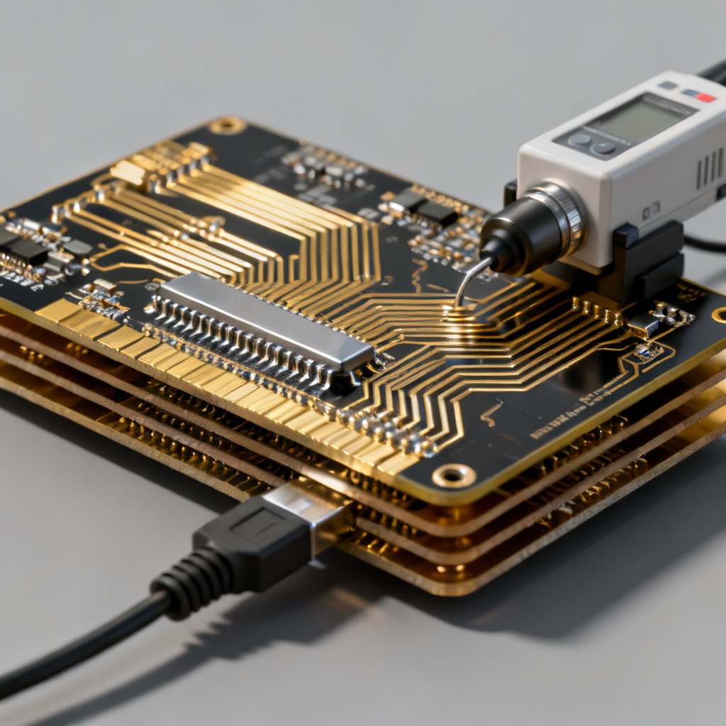
What is Periodic Jitter in High Speed PCB?
Periodic jitter (PJ) is a deterministic, bounded timing deviation that repeats at a fixed frequency. Unlike random jitter (RJ), which follows a Gaussian distribution and is unbounded, PJ is predictable and appears as distinct spectral peaks. In high speed PCB environments, the most common source is the switching noise from voltage regulators.
Core Definition of Periodic Jitter
Periodic jitter refers to the cyclical deviation of a signal’s transition edge from its ideal position in time, repeating at a constant rate. This periodicity directly links to a deterministic aggressor, such as a switching power supply’s fundamental frequency or its harmonics.
How It Differs from Other Jitter Types
Understanding jitter taxonomy is essential. Random jitter (RJ) is caused by thermal or shot noise and is unbounded. Data-dependent jitter (DDJ) results from intersymbol interference (ISI) due to channel losses. Periodic jitter (PJ) is caused by a deterministic, periodic noise source like a switching regulator. PJ is particularly dangerous because it can be mistaken for RJ during measurement, leading to overestimation of a system’s timing budget. Furthermore, PJ can cause specific bit error patterns; if the jitter frequency aligns with a clock recovery loop’s bandwidth, it can cause cycle slips.
Root Cause: How Switching Power Supplies Inject Timing Error
Switching power supplies (SMPS) are efficient but inherently noisy. They inject periodic jitter into high speed PCB signals through several well-defined mechanisms.
Switching Action: Ripple and Transients
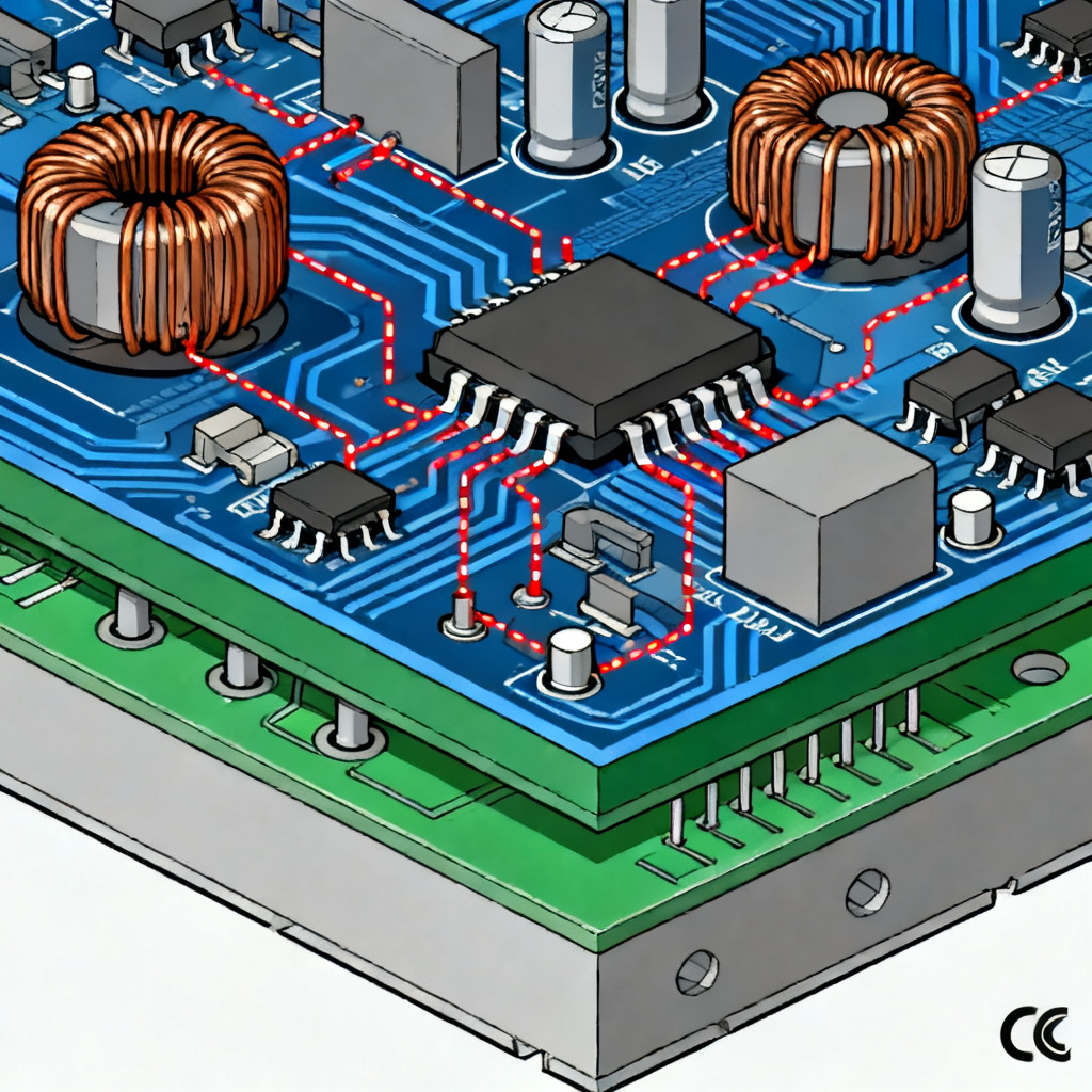
A typical buck or boost converter switches a MOSFET rapidly, creating output voltage ripple at the switching frequency (typically 100 kHz to 5 MHz) and high-frequency ringing from switching transients. This ripple directly modulates the supply voltage of high-speed buffers or PLLs. The primary mechanism is AM-to-PM conversion: a change in supply voltage alters the transistor switching threshold, causing the output edge to occur slightly earlier or later. For example, a 10 mV ripple at 1 MHz on a 1.8V supply can cause 1-2 ps of periodic jitter on a 10 Gbps signal, depending on the driver’s PSRR.
Ground Bounce and Return Path Discontinuities
SMPS draw large, pulsed currents, creating ground bounce across the ground plane. This voltage difference shifts the signal’s threshold relative to local ground, directly translating to timing error. Multiple switching regulators sharing the same ground plane can create a complex, multi-frequency ground noise spectrum, leading to PJ at multiple frequencies.
Magnetic Field Coupling (Inductive Crosstalk)
The SMPS inductor generates a time-varying magnetic field that induces voltage in nearby high-speed trace loops. This induced voltage shifts the signal’s zero-crossing point, injecting periodic jitter. The coupling is strongest when signal traces run parallel to the inductor in close proximity.
Capacitive Coupling (Parasitic Capacitance)
The SMPS switching node experiences high dV/dt. Through parasitic capacitance to a nearby signal trace, displacement current is injected, creating a voltage glitch that can cause false transitions or timing shifts.
Measuring SMPS-Induced Periodic Jitter
Identifying SMPS-induced periodic jitter requires specific measurement techniques.
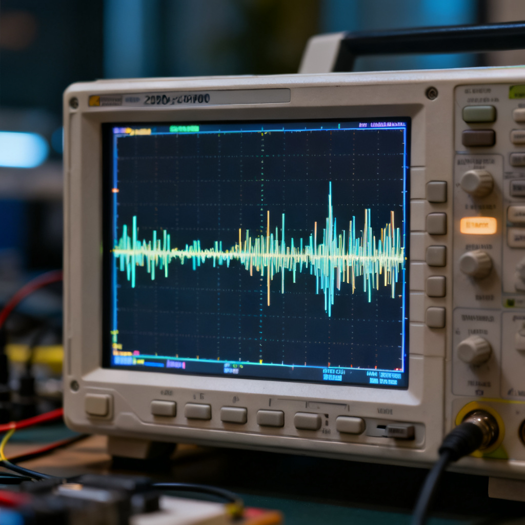
Time-Domain Measurement: Eye Diagram and Histogram
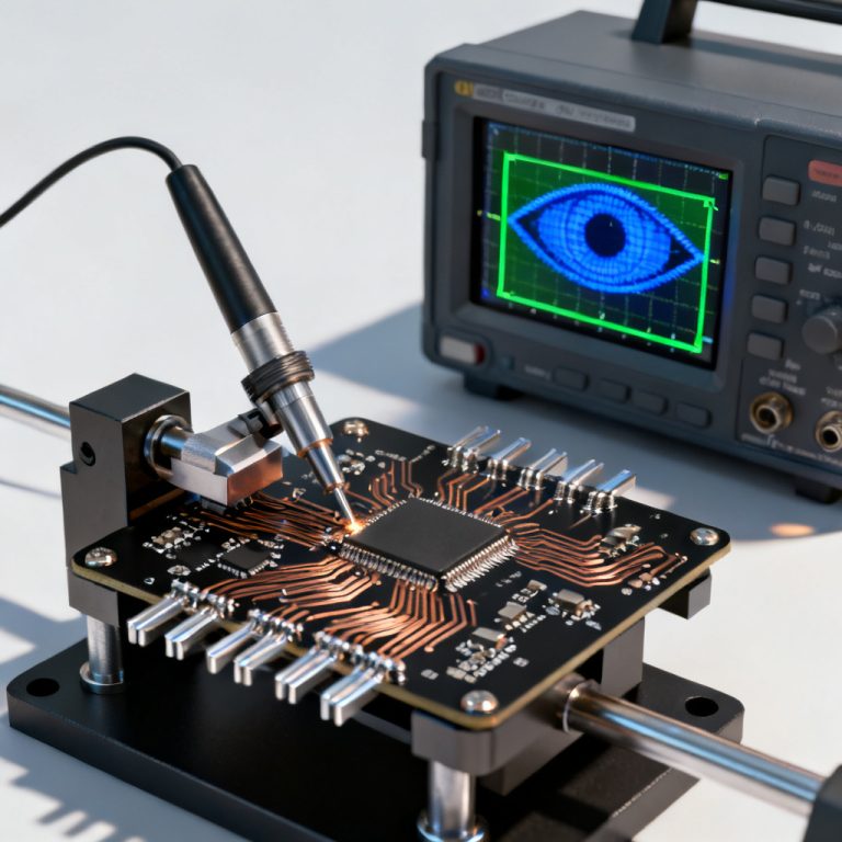
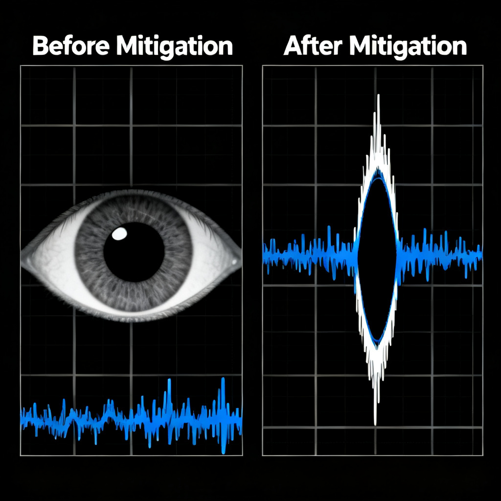
An eye diagram showing a “double-edged” or “fuzzy” eye closure that is not Gaussian often indicates PJ. A jitter histogram will show multiple peaks (multi-modal distribution) instead of a single Gaussian bell curve, with spacing corresponding to the jitter period.
Frequency-Domain Measurement: Phase Noise and Spectrum
A phase noise plot is the most powerful tool. It will show a clean carrier with discrete spurs at the switching frequency and its harmonics. Using a real-time oscilloscope with jitter analysis software, you can perform a Fourier transform on jitter vs. time data; PJ appears as distinct spikes in the frequency domain.
Identifying the Source: Correlation and Probing
If a jitter spur is measured at 500 kHz and the SMPS switches at 500 kHz, the cause is almost certain. Probe the power rail with a low-inductance probe and compare the ripple waveform with the jitter histogram. Trigger the oscilloscope on the SMPS switching node and observe the jitter locked to the SMPS period.
Mitigation Strategies for Periodic Jitter in High Speed PCB
Eliminating SMPS-induced periodic jitter requires a holistic approach across power design, PCB layout, and component selection.
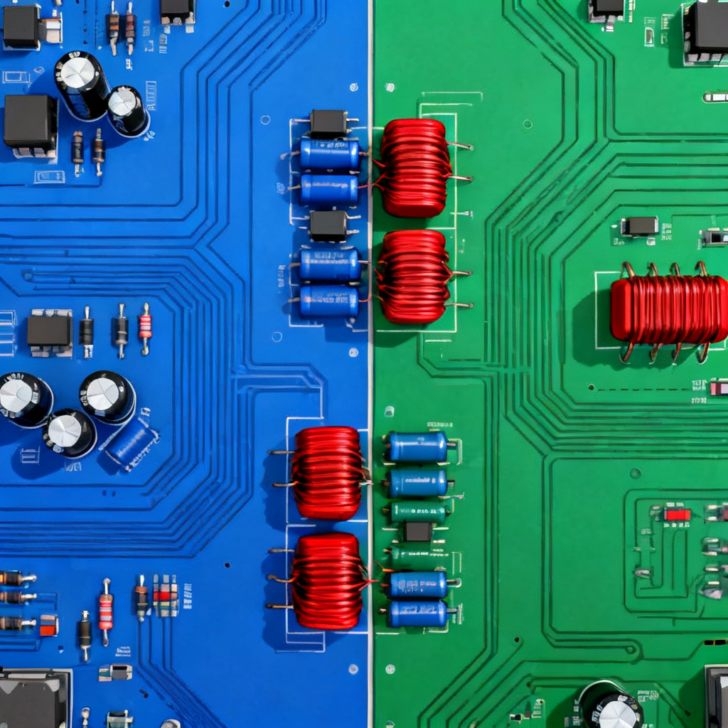
Power Supply Design Improvements
Increase switching frequency to push ripple and noise to a higher band, making filtering easier and placing noise outside PLL bandwidth. Use low-noise regulators like LDOs after the SMPS for excellent PSRR. Spread spectrum modulation (SSM) spreads jitter energy over a wider band, reducing peak amplitude.
PCB Layout Best Practices
Isolate power and signal grounds using split planes or a single-point connection. Minimize the hot loop (input capacitor, MOSFET, inductor) to reduce EMI and ground bounce. Physical separation of at least 1-2 inches between SMPS and high-speed traces is critical. Use shielding cans over the SMPS section if separation is impossible. Route SMPS output to a dedicated power plane through a ferrite bead or pi-filter.
Decoupling and Filtering
Use multi-stage filtering with bulk capacitors, mid-frequency MLCCs, and high-frequency MLCCs in parallel. Place ferrite beads in series with the power rail, choosing beads with high impedance at the SMPS switching frequency. Position the smallest, highest-frequency capacitors closest to IC power pins with multiple vias to reduce loop inductance.
IC-Level Mitigation
Select ICs with high PSRR across the SMPS frequency range. Many modern high-speed ICs have on-chip LDOs that provide additional filtering; ensure proper external decoupling as recommended.
Case Study: 10 Gbps Serial Link Failure
Scenario: A 10 Gbps NRZ serial link fails BER tests. The eye diagram shows significant closure, and the jitter histogram reveals a multi-modal pattern.
Diagnosis: Phase noise measurement shows a clear spur at 1.2 MHz. The board uses a 1.2 MHz switching regulator for the SerDes core. Probing reveals 15 mVpp ripple at 1.2 MHz on the core rail. The root cause is SMPS ripple modulating the SerDes transmitter’s PLL, causing ~3 ps peak-to-peak periodic jitter.
Solution: Added a ferrite bead (600Ω @ 1 MHz) and 10 µF capacitor in series with the SerDes power rail. Added three 100 pF capacitors within 2 mm of the SerDes power pins. Result: ripple dropped to <2 mVpp, the phase noise spur was eliminated, and BER tests passed.
FAQ: Periodic Jitter in High Speed PCB
What is the main cause of periodic jitter in high speed PCB designs?
The most common cause of periodic jitter in high speed PCB designs is noise from switching power supplies, including output ripple, switching transients, and coupled magnetic or capacitive fields.
How can I measure periodic jitter from a switching power supply?
Use a phase noise plot to identify discrete spurs at the SMPS frequency, or a jitter spectrum from a real-time oscilloscope to see distinct spikes. Correlate the frequency with the SMPS switching frequency.
What is the best way to reduce periodic jitter from SMPS?
Combine multiple strategies: increase SMPS switching frequency, use LDOs for sensitive rails, implement spread spectrum modulation, physically separate SMPS from high-speed traces, and apply multi-stage decoupling with ferrite beads.
Can periodic jitter be completely eliminated?
While complete elimination is difficult, careful design can reduce periodic jitter to negligible levels for most high-speed applications, typically below 1 ps RMS.
Conclusion: Path to Jitter-Free High-Speed Design
Periodic jitter from switching power supplies is a predictable, deterministic problem solvable with careful design. By understanding coupling mechanisms—ripple, ground bounce, magnetic fields, and capacitive coupling—and implementing robust mitigation strategies, you can ensure your high speed PCB meets its timing budget. At [Your Company Name], we specialize in manufacturing high-speed PCBs with stringent power integrity and jitter control, supporting designs from 10 Gbps to 112 Gbps.
Comparison: Our Approach vs. Standard Practices
| Parameter | Standard Practice | Our High-Speed PCB Approach |
|---|---|---|
| Power Filtering | Single bulk capacitor | Multi-stage L-C-L pi-filter with ferrite bead |
| SMPS-to-Signal Separation | Minimal or no separation | ≥2 inches with optional shielding can |
| Ground Plane Strategy | Shared ground plane | Isolated quiet ground with star connection |
| IC Selection Guidance | No PSRR consideration | PSRR-optimized ICs with on-chip regulation |
| Jitter Testing | Basic eye diagram only | Phase noise and jitter spectrum analysis |
Glossary of Key Terms
- Periodic Jitter (PJ): Deterministic, bounded timing deviation that repeats at a fixed frequency, often caused by switching power supply noise.
- AM-to-PM Conversion: The process by which amplitude modulation (ripple) on a power supply is converted into phase modulation (jitter) on a signal.
- PSRR (Power Supply Rejection Ratio): A measure of how well a component attenuates power supply noise, typically expressed in dB.
- Spread Spectrum Modulation (SSM): A technique that varies the SMPS switching frequency to spread jitter energy over a wider bandwidth, reducing peak amplitude.
- Ground Bounce: Voltage differences across a ground plane caused by large, pulsed currents, leading to timing errors in high-speed signals.