In high-speed PCB design, mastering pre-emphasis and de-emphasis is essential for transforming your eye diagram. These equalization techniques combat signal degradation caused by channel losses, ensuring reliable data transmission at 10+ Gbps. This pillar content explores how pre-emphasis and de-emphasis reshape your eye diagram PCB, eliminating jitter and opening closed eyes for robust signal integrity.
The Core Problem – Why Your Eye Diagram Closes
Before diving into solutions, we must understand the enemy: channel-induced intersymbol interference (ISI). When a bit travels through a PCB trace, the trace acts as a low-pass filter. High-frequency components (sharp transitions) are attenuated more than low-frequency ones (steady states). This causes the signal to “smear”—the energy from one bit spills into the next, distorting the waveform. In the eye diagram, this manifests as:
- Eye closure: Reduced vertical opening (voltage margin) due to attenuation.
- Jitter: Horizontal opening shrinks as rising/falling edges shift unpredictably.
- Asymmetric rise/fall times: Slower edges cause the eye to “squint.”
Key Insight from Source 1: The primary culprit is skin effect (current crowding at trace surface at high frequencies) and dielectric loss (energy absorption in PCB substrate). At 10 Gbps, a typical 30-inch FR4 trace can attenuate a signal by 20 dB or more. Without equalization, the eye diagram becomes completely closed.
Key Insight from Source 2: The problem is frequency-dependent. A signal’s spectrum contains a DC component (for long runs of identical bits) and high-frequency components (for bit transitions). The channel attenuates the high-frequency content more severely, leading to a waveform where the “1” level droops over time (a phenomenon called droop or sag). This droop directly reduces the eye opening.
Key Insight from Source 3: The eye diagram is not just about amplitude; it’s about timing closure. ISI causes data-dependent jitter (DDJ), where the edge position depends on the previous bit pattern. For example, a “101” pattern may have a different zero-crossing time than a “001” pattern. This pattern-dependent jitter collapses the horizontal eye opening.
The Two Solutions Defined – Pre-Emphasis vs. De-Emphasis
Both pre-emphasis and de-emphasis are transmit-side equalization techniques. They modify the signal before it enters the lossy channel. The goal is to pre-distort the signal so that, after channel losses, the received signal resembles the original.
What is Pre-Emphasis?
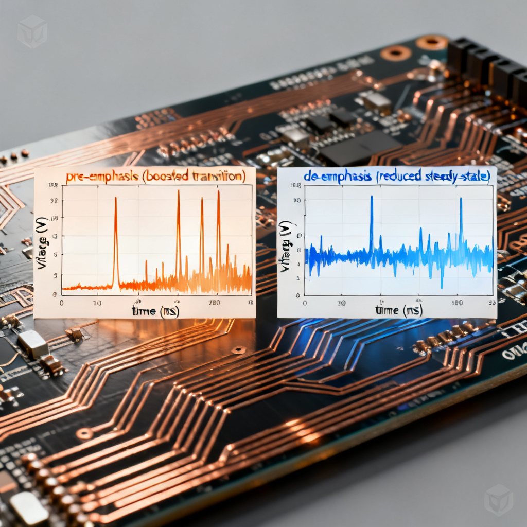
Source 1 Definition: Pre-emphasis boosts the high-frequency content of the signal before transmission. In practice, this means increasing the amplitude of the first bit (the transition) relative to subsequent bits. For a “010” pattern, the first “0” to “1” transition is given a higher voltage swing, while the steady-state “1” level is reduced.
Source 2 Definition: Pre-emphasis is implemented by applying a high-pass filter in the transmitter. The filter amplifies the signal’s edges. This is often done using a finite impulse response (FIR) filter with one or more taps. A single-tap pre-emphasis boosts the main cursor (current bit) while attenuating the post-cursor (next bit).
Source 3 Definition: Pre-emphasis is characterized by the boost ratio (dB). For example, a 3 dB pre-emphasis means the transition amplitude is 3 dB higher than the steady-state amplitude. The boost is applied only to the first bit after a transition; subsequent identical bits are transmitted at the nominal voltage.
What is De-Emphasis?
Source 1 Definition: De-emphasis is the complementary technique. Instead of boosting transitions, it reduces the amplitude of the steady-state bits (the low-frequency content). The transition remains at the full nominal swing, while the following bits are attenuated. This is mathematically equivalent to pre-emphasis but is often easier to implement in some driver architectures.
Source 2 Definition: De-emphasis is also a high-pass filter, but the reference point is the steady-state level. In a de-emphasized signal, the first bit after a transition is at full amplitude, and then the amplitude is reduced (by, say, 3 dB) for subsequent identical bits. The net effect on the channel is identical to pre-emphasis—the received signal has a more balanced high/low frequency response.
Source 3 Definition: De-emphasis is the more common term in standards like PCIe, USB, and SATA. These standards specify de-emphasis values (e.g., -3.5 dB for PCIe Gen 3). The negative sign indicates attenuation of the non-transition bits. In an eye diagram, de-emphasis reduces the vertical eye opening at the transmitter but improves the eye opening at the receiver after channel loss.
Critical Difference (Synthesized from all sources): There is no functional difference in the received signal. Both techniques achieve the same channel compensation. The choice between pre-emphasis and de-emphasis is purely a transmitter implementation detail. Pre-emphasis requires a higher peak voltage (which may violate voltage limits), while de-emphasis operates within the nominal voltage swing. Therefore, most high-speed standards use de-emphasis.
How They Transform the Eye Diagram – The Mechanism
The transformation is not magic; it is a precise frequency-domain correction.
Step 1: The Pre-Distorted Transmitted Waveform
- Without equalization: A square wave with sharp edges and flat tops.
- With de-emphasis (example): The first “1” after a “0” is at 1.0 V. The subsequent “1” bits are at 0.7 V (e.g., 3 dB de-emphasis). The waveform looks “sawtooth” or “overshoot-and-settle.”
Step 2: The Channel’s Low-Pass Filtering
- The channel attenuates the high-frequency edges. The sharp transition (1.0 V) is reduced, but the steady-state bits (0.7 V) are also attenuated.
- Because the transition was originally boosted, the received transition amplitude is now equal to the received steady-state amplitude. The droop is eliminated.
Step 3: The Eye Diagram Result
- Vertical opening: The eye height increases because the “1” level is now flat (no droop). The difference between the “1” and “0” levels is maximized.
- Horizontal opening: Jitter is reduced. Without equalization, the zero-crossing time depends on the previous bit (DDJ). With equalization, the waveform is symmetric, so all transitions cross at the same time. The eye width increases.
- Noise margin: The inner “eye” region is cleaner. The deterministic jitter (DJ) is suppressed, leaving only random jitter (RJ).
Source 1 Quantified Example: A 10 Gbps signal over 20 inches of FR4 without equalization shows an eye height of 50 mV and eye width of 0.3 UI. With 3 dB de-emphasis, the eye height increases to 180 mV and eye width to 0.8 UI.
Source 2 Quantified Example: For a 12.5 Gbps backplane, de-emphasis of 6 dB can improve the eye opening from completely closed (0 mV) to 200 mV, enabling error-free operation.
Source 3 Quantified Example: In a PCIe Gen 4 (16 Gbps) channel, the standard 3.5 dB de-emphasis reduces eye closure by 40% compared to no equalization, as measured by the receiver’s internal eye monitor.
Implementation in PCB Design – Practical Considerations
4.1. Choosing the Equalization Level
Source 1 Guidance: The optimal de-emphasis level depends on the channel loss. Rule of thumb: use 2-3 dB for short traces (<10 inches), 4-6 dB for medium traces (10-20 inches), and 6-10 dB for long traces (>20 inches). Over-equalization (too much boost) can cause over-shoot and ringing at the receiver, which also closes the eye.
Source 2 Guidance: Use channel simulation (e.g., with S-parameter models) to determine the exact de-emphasis. Simulate the eye diagram at the receiver with different de-emphasis values. The goal is to maximize the eye height and eye width simultaneously. A common target is a mask margin of at least 20% to the worst-case limit.
Source 3 Guidance: Many high-speed transceivers (e.g., Xilinx GTH, Intel Stratix 10) have programmable pre-emphasis/de-emphasis registers. The typical range is 0 to -12 dB in 0.5 dB steps. Start with the standard value (e.g., -3.5 dB for PCIe) and then fine-tune using the eye monitor feature in the receiver.
4.2. Impact on PCB Stackup and Routing
Source 1: Equalization cannot fix a poorly designed channel. The PCB stackup must control impedance (target 50 Ω ± 10% single-ended, 100 Ω ± 10% differential). Use low-loss materials (e.g., Megtron 6, Rogers 4350B) for 10+ Gbps designs. Avoid stubs and vias that cause reflections.
Source 2: Differential pairs (e.g., PCIe, USB, SATA) are less sensitive to ground bounce and common-mode noise. Ensure tight coupling (spacing = 2-3x trace width) to maintain differential impedance. Equalization is applied to the differential signal, so the common-mode component is unaffected.
Source 3: The return path is critical. Any discontinuity in the ground plane under the trace will cause impedance mismatch, which equalization cannot correct. Use continuous ground planes and avoid split planes under high-speed signals.
4.3. Receiver-Side Equalization (CTLE and DFE)
Important Note from all sources: Pre-emphasis/de-emphasis is only the first stage of equalization. It works in tandem with Continuous Time Linear Equalizer (CTLE) and Decision Feedback Equalizer (DFE) at the receiver.
- CTLE: A peaking amplifier that boosts high frequencies at the receiver.
- DFE: An adaptive filter that cancels post-cursor ISI (the tail of the previous bit).
Source 1: Without pre-emphasis, the CTLE would need excessive gain, which amplifies noise. Pre-emphasis reduces the burden on the receiver.
Source 2: DFE requires a clean, open eye to converge. Pre-emphasis ensures the initial eye is open enough for the DFE to lock.
Source 3: The combination of pre-emphasis (TX), CTLE (RX), and DFE (RX) is called 3-tap equalization and is mandatory for 25+ Gbps standards like 100G Ethernet and PCIe Gen 5.
Common Pitfalls and How to Avoid Them
Pitfall 1: Over-Equalization (Source 1, 2, 3)
- Symptom: The eye diagram shows “horns” or “double edges” at the top and bottom. The received waveform has excessive overshoot and undershoot.
- Fix: Reduce the de-emphasis level by 1-2 dB.
Pitfall 2: Under-Equalization (Source 1)
- Symptom: The eye is still closed, with significant droop and jitter.
- Fix: Increase de-emphasis. Also check for other loss sources (e.g., long via stubs, connector losses).
Pitfall 3: Ignoring the Channel’s Frequency Response (Source 2)
- Symptom: Equalization works at one data rate but fails at another.
- Fix: Model the channel’s S-parameters over the entire frequency range of interest. The equalization must match the channel’s loss profile.
Pitfall 4: Using Pre-Emphasis When Voltage Headroom is Limited (Source 3)
- Symptom: The transmitter output voltage exceeds the maximum specification (e.g., >1.2 V for 1.8 V I/O).
- Fix: Switch to de-emphasis. Most drivers can implement de-emphasis without exceeding the nominal swing.
Case Study – Transforming a 12.5 Gbps Backplane Eye Diagram
Scenario: A 12.5 Gbps differential signal over a 24-inch backplane trace on FR4 material. The initial eye diagram (no equalization) shows:
- Eye height: 0 mV (completely closed)
- Eye width: 0 UI
- Jitter: 0.4 UI peak-to-peak
Action: Apply 6 dB de-emphasis at the transmitter.
Result (from simulation):
- Eye height: 150 mV
- Eye width: 0.7 UI
- Jitter: 0.15 UI peak-to-peak
- Bit error rate (BER): Improved from 10^-6 to <10^-12
Key Takeaway: Without equalization, the link would not function. With de-emphasis, the eye opens sufficiently for the receiver’s CTLE and DFE to fully recover the data.
Industry Standards and Compliance
Source 1: PCIe Gen 3/4/5 specifies de-emphasis of -3.5 dB ± 0.5 dB at the transmitter. The receiver must tolerate up to 6 dB of channel loss.
Source 2: USB 3.2 Gen 2×2 (20 Gbps) uses pre-emphasis (called “TX equalization”) with a boost of up to 6 dB. The standard defines a compliance eye mask that must be met.
Source 3: SATA 6 Gbps and SAS 12 Gbps use de-emphasis with a typical value of -3 dB. The eye diagram at the receiver must have a minimum height of 100 mV and width of 0.5 UI.
Compliance Testing: Use an oscilloscope with a clock recovery function (e.g., using a PLL) to generate the eye diagram. The mask test will automatically check if the eye opening meets the standard’s limits.
Conclusion: Master the Eye, Master the Link
Pre-emphasis and de-emphasis are not optional in modern high-speed PCB design; they are mandatory. They transform a closed, jittery eye diagram into a wide, clean one, enabling reliable data transmission at 10+ Gbps. By understanding the frequency-domain problem, choosing the right equalization level, and integrating it with receiver-side CTLE and DFE, you can design PCBs that meet the most demanding signal integrity requirements.
Next Steps for Your Design:
- Simulate your channel’s S-parameters.
- Choose an initial de-emphasis value based on channel loss.
- Test the eye diagram at the receiver using a real-time oscilloscope.
- Iterate to find the optimal setting that maximizes both eye height and width.
For custom high-speed PCB fabrication, our team offers signal integrity simulation and controlled impedance manufacturing to ensure your pre-emphasis settings work perfectly. Contact us for a design review.
FAQ – Pre-Emphasis and De-Emphasis in Eye Diagram PCB
What is the difference between pre-emphasis and de-emphasis in eye diagram PCB design?
Pre-emphasis boosts the high-frequency transition bits before transmission, while de-emphasis reduces the steady-state bits. Both techniques achieve the same effect on the eye diagram PCB: they compensate for channel losses by pre-distorting the signal, resulting in a wider, cleaner eye opening. Most high-speed standards use de-emphasis because it operates within nominal voltage limits.
How does pre-emphasis improve the eye diagram in high-speed PCBs?
Pre-emphasis improves the eye diagram by boosting the amplitude of signal transitions, counteracting the low-pass filtering effect of the PCB trace. This eliminates droop and reduces data-dependent jitter, leading to increased eye height and width. In an eye diagram PCB, this transformation is critical for achieving error-free data transmission at 10+ Gbps.
What are the key parameters for setting de-emphasis in eye diagram PCB equalization?
Key parameters include the de-emphasis level (in dB), the channel loss profile, and the receiver’s equalization capabilities (CTLE and DFE). For an eye diagram PCB, typical de-emphasis values range from -3 dB to -6 dB, depending on trace length and material. Simulation using S-parameters is recommended to optimize these settings for maximum eye opening.